High-Speed PCB Design

What Is High-Speed PCB Design
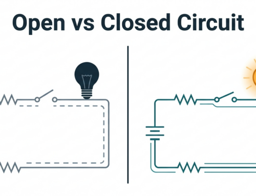
High-speed PCB design describes designing high-speed signals on a printed circuit board (PCB).
High-speed signals normally have rise and fall times of less than one split second (ns).
It involves expertise of signal integrity for high speed layout, electro-magnetic compatibility,
impedance matching, stacking design, electrical wiring rules, etc.
The purpose of high-speed PCB design is to make certain the quality and reliability of high-speed
signals and stay clear of problems such as signal distortion, interference, and representation.
High-Speed PCB Design Considerations
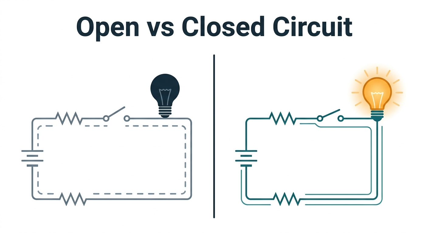
1) Impedance Matching
High-speed signals will create electromagnetic fields throughout transmission.
If the signal does not match the resistance of the transmission line, this can result in signal
representations, which can degrade signal efficiency.
2) Spacing
The transmission of high-speed signals will be interfered with by other signals, source of power, ground
lines, etc. Boosting the spacing between signals can lower interference.
3) Length Matching
Both lines of the differential signal should have the same size. If the lengths are various, it will
create signal inconsistency, hence reducing signal stability.
High-speed PCB design requires specialized tools and techniques to make sure signal honesty for high
speed design.
Specialized tools can help developers examine signal transmission paths and recognize possible problems.
Advantages of High-Speed PCB Style
1) Maximize Signal Transmission Performance
High-speed PCB design can optimize signal transmission efficiency, causing lower signal loss and less
interference at high frequencies, thus boosting system dependability and security.
2) Signal Integrity
With accurate design and layer stack design, signal reflection, crosstalk, clock jitter, and other
problems can be prevented to guarantee signal top quality and integrity.
3) Power Optimization
High-speed PCB style can reduce power loss and improve system efficiency by maximizing circuit format
and layer stack style, which is specifically essential in mobile devices and battery-powered systems.
4) Enhanced Warmth Dissipation
For high-power digital devices, a precise broadband PCB design can enhance heat dissipation and ensure
the security of digital elements under high-load operation.
5) Reduced Design Cycle
Adopting advanced design devices and simulation innovation can increase the design procedure, reduce the
product growth cycle, and improve market competition.
Application of High-Speed PCB
Below are some details application instances:
1) Digital Signal Processing
Digital signal processing (DSP) describes the innovation of handling electronic signals.
DSP modern technology is extensively made use of in various electronic items, such as sound and video
processing, picture processing, interaction, etc.
High-speed PCB design is vital in DSP applications since DSP systems normally require to transfer
high-speed signals.
In sound and video clip processing systems, high-speed PCBs are utilized to send audio and video clip
signals.
2) Interaction
Interaction systems usually need to transmit high-speed signals, such as in Ethernet, fiber optic
interaction, wireless interaction, and various other systems.
High-speed PCB design is considerable in interaction systems to make sure signal stability and
dependability.
3) Storage
Storage systems are typically made use of in solid-state drives (SSDs), memory, and flash storage space.
For example, in an SSD, a high-speed PCB is made use of to transfer information signals.
In memory, high-speed PCB is used to send data signals.
In flash memory, high-speed PCB is utilized to transmit data signals.
4) Picture Handling
Such as electronic cameras, scanners, displays, etc.
High-speed PCB design is essential in photo handling applications because image processing systems
usually need to send high-speed signals.
As an example, in digital cameras, high-speed PCBs are used to send picture signals.
In scanners and screens, high-speed PCBs are utilized to send picture signals.
Summary
High-speed PCB design is a complicated job that calls for considerable knowledge.
With proper design and implementation, you can ensure that high-speed PCBs can efficiently beam and
fulfill system needs.
