High-Volum PCB Manufacturing

Electronic products are gradually altering our lives. As our dependancy on digital products rises, it
indicates that we require massive PCB and PCB assembly to meet the demand. It is essential to choose a
strong large-scale supplier when you require massive circuit card production.
This post will certainly present the high-volume PCB manufacturing procedure to everybody to ensure that
everybody can comprehend how to produce high-volume printed circuit card and our PCB manufacturing
abilities.
What is High-Volume PCB Manufacturing?
High-volume PCB production refers to the process of a producer producing greater than 1,000 printed
circuit boards in the exact same time cycle. Numerous automated mechanical tools are utilized in the
manufacturing procedure to allow these circuit card to be manufactured successfully and keep PCB useful
consistency and uniform look.
Advantages of Mass Production of PCBs
There are many benefits to making use of automation in PCB production, such as expense savings,
shortened shipment time, enhanced manufacturing performance, etc. Allow’s take a more detailed look!
• Lowered Prices
This advantage is just one of the reasons why most individuals choose high-volume PCB manufacturing. The
primary method to minimize production prices is with economies of range and lower manufacturing costs.
Manufacturers lower expenses by acquiring PCB basic materials in bulk and utilizing large manufacturing
equipment to enhance job efficiency.
• Reduced Time Cycle
When producing PCBs in huge quantities, manufacturers will set up special devices and procedures to
optimize massive production. Considering that the production procedure is completely automated, you will
certainly save PCB manufacturing time, and the product can be offered as soon as possible, which is a
benefit in the electronic devices field.
• Quality Control
Because the circuit card are mass-produced, it can guarantee the constant top quality of all PCB boards.
You don’t require to fret about the high quality distinction between one board and others. During
the manufacturing procedure, the motherboard are examined and checked to guarantee they fulfill the
performance demands.
• Enhance Market Competition
High-volume printed circuit card manufacturing conserves time for succeeding high-volume PCB assembly.
It can assist you accelerate time to market and fulfill high mart needs on schedule. Combined with
expense reduction, it likewise aids to improve market competitiveness and go beyond competitors.
High-Volume PCB Production Process
• Cutting
Cutting is cutting the initial copper-clad laminate into boards made on the production line.
Initially, allow us recognize a couple of principles:
1) Unit: Unit refers to the unit graphics designed by PCB design engineers.
2) Set: Set refers to the graphics in which designers place multiple units to boost
efficiency and facilitate manufacturing. We typically call it a panel, which includes device graphics,
procedure edges, and so on
3) Panel: Panel describes a board composed of multiple sets put together and added with
device board edges to improve efficiency and promote production when PCB suppliers create.
• The Inner Layer Of Dry Film
Inner layer of dry film is the process of moving the internal layer circuit graph to the PCB board.
Inner layer of dry film consists of a great deal of procedures, such as inner layer movie pasting,
direct exposure and growth, and internal layer etching.
Internal layer film pasting is a certain photosensitive movie externally of the copper plate, which we
commonly call the dry film. This film will strengthen when revealed to light, forming a protective movie
on the board.
Exposure and development are to expose the board with the film pasted, and the light-transmitting part
will be solidified, while the non-light-transmitting part will still be a dry film. Then development,
the uncured dry film is removed, and the board with the cured protective film is etched. After the film
is removed, the inner layer circuit pattern is transferred to the board.
• Browning
Function: To develop microscopic roughness and natural steel layer on the inner copper surface area to
boost the bonding toughness between layers.
Principle of the process: Via chemical therapy, create an uniform organic steel layer framework with
good bonding buildings, make the surface of the copper layer roughen before the internal layer is bound,
which is used to improve the bonding strength in between the inner copper layer and the semi-cured sheet
after pushing.
• AOI Examination
This step is significant. When the layer and layer between are assembled, the errors in the inner layers
can not be transformed. The AOI machine will certainly contrast it with the initial design and discover
any kind of problems that will be shown on the screen. PCB with problems will be eliminated at this
stage.
• Lamination
Lamination is bonding each layer of the circuit right into a whole making use of the adhesiveness of the
PP sheet. Copper aluminum foil, bonding sheet (prepreg), internal layer board, stainless-steel,
isolation board, kraft paper, outer layer steel plate, and various other materials overlap according to
the process needs.
• Drilling
Develops via- holes in between layers of the motherboard to link the layers.
• Copper Plate Plating
1) Copper Deposition
It is likewise called chemical copper after the PCB board exploration undergoes an oxidation-reduction
response in the copper deposition storage tank to develop a copper layer to metalize the hole to make
sure that copper is transferred externally of the initial insulating substratum to accomplish an
electrical link in between layers.
2) Plate Plating
The copper on the surface and inside the holes of the newly copper-plated PCB is enlarged to 5-8um to
stop the thin copper inside the holes from being oxidized and micro-etched prior to pattern
electroplating, hence revealing the substratum.
• Outer Dry Film
The procedure coincides as the internal dry film.
• External Layer Pattern Plating and SES
The copper layer of openings and circuits is plated to a bound thickness (20-25um) to meet the copper
density demands of the final PCB board. The extra copper on the board is engraved away to disclose the
practical circuit pattern.
• Solder Mask
Solder masks, additionally referred to as eco-friendly oil, are one of the most vital processes in
printed circuit board manufacture. It safeguards copper. It is used with a layer of solder mask on the
panel by screen printing or finishing with solder mask ink. After direct exposure and growth, the pads
and holes to be soldered are subjected, and other locations are covered with solder masks to avoid short
circuits during welding.
• Silkscreen
Silkscreen is a way to affix a calling card or label to a circuit card. Utilize an inkjet printer to
print info directly on the circuit card. The details includes company ID, symbol, element number, etc.
It is exposed to the panel by ultraviolet light.
• Surface Area Therapy
Bare copper has excellent solderability, yet it is easily oxidized by dampness when revealed to air for
a very long time. It tends to exist in the form of oxides and is unlikely to remain as initial copper
for a long period of time. For that reason, the copper surface area requires to be surface-treated. The
most standard objective of surface area therapy is to make sure excellent solderability or electrical
residential or commercial properties.
Usual surface treatments are spraying tin, immersion gold, OSP, immersion tin, immersion silver, nickel
palladium gold, electrical hard gold, electric gold fingers, etc –
• Forming
Utilize a cutting machine to cut the PCB right into the wanted size.
PCB Scoreboard mostly includes V-shaped scribing, lug circuitry, transmitting, laser Scoreboard, etc –
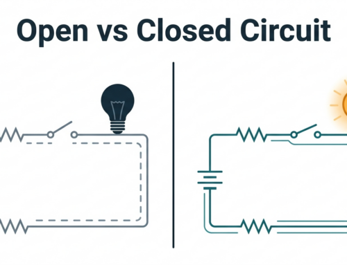
Electrical Test
Copy the standing of the PCB board, power it on to check the electrical performance, whether there is an
open circuit or short circuit.
• Final Inspection
Check the look, dimension, opening size, density, marking, and so on, to guarantee the PCB board
satisfies client needs. Load certified products into packages for easy storage space and transport.
Technical Development And Advancement
To fulfill market need, PCB makers will certainly present several advanced PCB production devices to
allow mass PCB manufacturing to be executed efficiently and organized while high volume PCB boards.The
significant PCB production devices is as complies with:
• Automated Photolithography Device
The photolithography device is likewise called a mask positioning direct exposure maker.
Photolithography technology is essential in PCB production. It can quickly and effectively move circuit
patterns to the surface area of photosensitive products and afterwards form PCB patterns that meet
layout needs with chain reaction. With the continual growth of scientific research and innovation, the
resolution of photolithography makers has actually gotten to the nanometer degree, offering considerable
support for the development of electronic technology.
• Automated Etching Machine
Engraving eliminates unneeded copper on the PCB. The automated etching machine can accurately understand
the etching speed and level.
• Automated Screening Devices
Automated testing devices, such as AOI and X-ray, detect high quality defects and performance barriers
of PCB boards and make certain the manufacturing of top quality and high-performance PCBs.
• Exploration Device
Modern exploration machines have the attributes of multi-drilling, high-precision boring, automated
control exploration, and quickly device adjustment, making the boring procedure a lot more precise and
fast. Modern PCB drilling machines can boost PCB production effectiveness and satisfy the manufacturing
requirements of high-density PCB boards.
High-Volume PCB Production Applications
High-volume PCB production is critical in different areas. It can generate a multitude of reputable and
high-grade printed circuit board. High-volume PCB production is mainly utilized in the adhering to
aspects:
• Customer Electronics
In the customer electronics sector, massive PCB manufacturing can fulfill the high market demand for
mobile phones, tablets, and others and ensure the high quality of PCBs.
• Automotive Market
In the automobile industry, with the growth of electric vehicles and independent driving technology, the
role of PCB in automotive electronics is ending up being progressively essential. In the automation
control system, the PCB is the control center responsible for signal transmission and processing.
• Communication
Smart phone, base stations, and other telecom devices count on circuit card. Large manufacturing
capacities assist satisfy the high need for these gadgets.
Present Standing Of Mass PCB Production
Huge PCB manufacturing is an extremely specialized and technology-intensive procedure. It needs
producers to have progressed equipment, specific procedure circulation, and stringent quality assurance.
Currently, numerous factories have recognized completely automated production lines, using equipment
that enhances manufacturing effectiveness, such as robot arms, automated punching devices, laser
inscription devices, etc. Furthermore, computer-aided design (CAD) software has dramatically sped up the
rate of PCB design, while computer-aided manufacturing (CAM) ensures the accurate improvement of designs
into real items.
Challenges
In spite of the continuous innovation of innovation, mass PCB manufacturing still faces a series of
challenges. First, the adjustment in resources costs creates anxiety on producers’ profit margins.
Second, with the sped up speed of digital item replacement, PCB style and manufacturing cycle need to be
shortened. On top of that, the environmental policies require the PCB manufacturing process to be much
more green and eco-friendly, which puts greater requirements onward in the manufacturing process.
Technology Under Sector 4.0
Market 4.0 has brought new possibilities for PCB production. Through the Internet of Things (IoT) modern
technology, manufacturing tools can be adjoined, production condition can be kept track of in real time,
and upkeep demands can be predicted, consequently lowering downtime and boosting production efficiency.
Using huge information evaluation and artificial intelligence can enhance the production process and
attain the ideal arrangement of resources. On top of that, wise manufacturing can likewise supply
tailored PCBs to meet the marketplace need for small batches and diversity.
Future Overview
High-volum PCB manufacturing will remain to establish in the direction of automation and intelligence.
With the popularization of 5G interaction innovation, the design and manufacture of PCBs will certainly
pay even more interest to high-frequency and high-speed transmission performance. At the same time,
sustainable development will end up being a considerable issue in the sector. Exactly how to achieve
green production while guaranteeing efficiency will certainly be a trouble that makers need to fix. In
addition, with the rise of adaptable digital modern technology, future PCBs might be thinner and extra
versatile, opening up a lot more possibilities for ingenious applications.
