PCB Fundamentals – PCB Manufacturing, PCB Terminology

Printed circuit boards are a crucial part of digital tools. When many people hear this word, they really
feel that they have actually touched an understanding blind spot and know nothing about PCB. As a
result, this article will quickly describe PCB to ensure that everyone can recognize printed printed
circuit board and some PCB professional terms.
What Is a PCB?
PCB can also be called printed wiring board (PWB). In specialist terms, PCB refers the carrier for the
electric connection of digital parts and is additionally the support of digital parts. In basic terms,
PCB is an area to place electronic components to ensure that these digital elements are attached to
create a circuit.
Classification of PCB
Printed circuit boards can be separated right into various PCBs according to different characteristics.
According to the stamina of the substrate, it can be separated right into rigid PCB (rigid printed
circuit board), flex PCB, rigid-flex printed circuit board, etc.
According to the base material, it can be divided into Steel core PCB and FR4 PCB.
According to layers, it can be divided into single-layer PCB, double-layer PCB, multi-layer PCB, and
high-density interconnect board (HDI).
1) Single-Layer PCB
Single-layer boards are the simplest boards. One side is utilized for transmitting on the circuit board,
and the various other is used to install digital parts and print logos.
Single-layer boards appropriate for simple circuit connections since it is tough to wire just one side.
The very best feature of single-layer boards is their affordable price and easy production procedure.
2) Double-Layer PCB
Double-layer boards can be transmitted on both sides of a protecting board, with one side as the leading
layer and the other as the bottom layer. The top layer and the bottom layer are electrical links with
vias.
Usually, digital elements are installed on the top layer. Nonetheless, to minimize the dimension of the
circuit board, parts can likewise be put on both layers.
The features of double-layer boards are moderate costs and very easy electrical wiring. It is the most
commonly made use of printed circuit board kind at present.
3) Multi-Layer PCB
Circuit card with greater than two layers.
4) High-Density Interconnect Board
Circuit board with high density making use of micro blind buried using technology. HDI is a small item
made for small-capacity users.
Structural Composition of PCB
PCB generally includes copper-clad laminates (CCL), prepreg (PP sheet), copper aluminum foil, and solder
masks. At the same time, to protect the revealed copper foil on the surface and guarantee the welding
effect, the PCB needs to be surface-treated and marked with characters (also known as silk screen
printing).
1) Copper-Clad Laminate
Copper-clad laminate (CCL) is the raw material in printed circuit board manufacturing. It is a composite
product composed of a dielectric layer (resin, glass fiber) and a high-purity conductor (copper foil).
FR4 is the most frequently used out there.
2) Prepreg
Prepreg, likewise called PP sheet, is just one of the primary products created by multi-layer boards. It
is generally composed of material and enhancing materials. Prepreg will soften under heating and stress
and strengthen after cooling down.
3) Copper Foil
Copper aluminum foil is a thin, constant metal aluminum foil on the base layer of the circuit card. It
is the conductive source of the PCB. It is easily bonded to the shielding layer and etched to create a
circuit pattern.
4) Solder Mask
Printing ink on the panel surface secures the copper. The ink is generally environment-friendly, so the
PCB boards that we see are eco-friendly. Naturally, we additionally can publish other shades of ink,
such as red, black, blue, and so on.
5) Silk Screen Printing
It is located on the top layer of the PCB board and is made use of to publish text notes, and so on. It
is equivalent to making a PCB tag.
What Are the Steps in PCB Manufacturing?
PCB construction begins with blueprint style and experiences several phases to obtain a complete PCB
product. Each step is significant because they are all related.
1) Design PCB
PCB developers usually make use of a software called Extended Gerber, which not only aids with the
design but also encodes info about the number of copper layers, solder mask layers, and various other
element signs.
Our PCB producer does not require to do PCB design. Since the PCB layout (Gerber documents) is supplied
by clients, Before production, the factory will perform a secondary problem examination, a procedure
called producing layout examination. After confirmation, the next action will certainly be executed:
design testimonial and engineering issues.
2) Layout Review and Design Concerns
This action is to check the design for omissions and errors. The PCB can be printed after the engineer
validates the layout has no problems or possible errors.
3) Publish PCB Design
The printing of the PCB layout makes use of a specific plotter. This printer publishes the PCB design as
something like film. Use two ink colors to suggest the internal and external layers of the PCB.
• Black Ink
The inner layers stand for the copper traces and circuits of the PCB; Black ink on the outer layers of
the PCB represents areas where copper has actually been gotten rid of.
• Transparent Ink
Used on the internal layer for non-conductive locations; on the outer layer to indicate copper vias.
Each PCB layer has a solder mask. The PCB has four layers, which require 8 sheets of black film. At the
same time, the movie requires a punched opening with a puncher to place it.
4) Printing Copper
This action notes the main beginning of PCB fabrication. The PCB design prints onto a laminate with
copper foil pre-bonded on each side. Then, the copper is etched away to reveal the blueprint of the
initial style.
Next off, tidy the copper. To guarantee the printed panel has no dust externally. Otherwise, it may
trigger a short or open circuit in the PCB.
A light-sensitive film, called photoresist, is applied to the tidy board. Photoresist contains a
chemical that sets when exposed to ultraviolet light.
Next off, the movie and printed circuit board are straightened with the positioning holes and placed
under ultraviolet light to solidify the photoresist. Ultimately, the unhardened locations of the circuit
card are cleaned with an alkaline solution and afterwards dried out.
5) Eliminate Excess Copper
In a similar way, we utilize an alkaline option to liquify the excess copper in the internal layer, and
the called for copper will not be affected under the photoresist solidifying layer. The moment required
for dissolution and the solvent are in favorable feedback with the weight and dimension of the circuit
card.
6) Alignment of Inner and Outer Layers
After cleaning, align the inner layer with the outer layer. Normally, the professional positions the
circuit board on a punching equipment called an optical puncher, and the machine straightens the inner
layer with the outer layer by passing pins with the placing holes.
7) Automatic Optical Inspection
This step is extremely substantial. When the layers are put together, the inquiry can not be fixed in
the inner layers. To guarantee the PCB isn’t faulty, professionals will use AOI inspection. The AOI
machine will contrast the PCB board with the original style. Some troubles will be shown on the screen.
Failing circuit boards will be disused at this phase.
8) Lamination PCB Layer
At this action, the PCB board is formed. The layers without issues are compressed. There are the
adhering to steps:
• Riveting
Rivet multiple inner core boards and films (prepregs) together to avoid inconsistency throughout
subsequent handling.
• Lamination
Pre-laminated boards are stacked in the form of multi-layer boards to be pressed in prep work for
pushing.
Under vacuum cleaner problems, the piled boards are pushed right into multi-layer boards by heating.
• Post-Processing
The laminated boards go through grinding, targeting, and milling for the initial profile treatment.
9) Drilling
PCB boring calls for high accuracy due to the fact that a little mistake can lead to hefty financial
loss. Use an X-ray device to locate the drill openings to make sure that you locate the appropriate
drill location.
Before drilling, workers need to put buffer material under the drilling target to ensure the cleanness
of the drilling. The positioning hole is to deal with the PCB. When drilling, the computer will
control the drill little bit to identify the suitable boring placement with the Gerber design data as
the target. As soon as drilling is total, eliminate the continuing to be copper on the edge.
10) PCB Plating
After a series of chain reactions, a slim layer of copper is deposited on the wall surface of the
pierced opening.
11) External Imaging
Apply photoresist and use yellow light for lighting, as photoresist solidifies under UV light. Usage
pins to deal with the black clear movie to avoid it from being misaligned with the panel.
Like step 4, carried out in a clean and sterile environment, we additionally utilize ultraviolet light
on the external layer to set the photoresist. The panel enters the mashine to remove the unhardened
photoresist shielded by the black ink.
12) Outer Layer Etching
The photoresist is liquified and cleansed to get rid of the excess copper. An alkaline solvent liquifies
excess copper foil in preparation for AOI inspection and soldering.
13) External Layer AOI Inspection
Like the internal layer, the outer layer additionally needs to undertake automated optical inspection to
make certain that the procedure of this layer fulfills the layout demands. It can additionally check
whether excess copper has been gotten rid of from the previous layer.
14) Solder Mask
Initially, clean the circuit board to get rid of contaminations or excess copper.
The board surface is used with ink and a solder mask. The PCB is subjected to ultraviolet light to
harden the photosensitive film and get rid of the unhardened components.
The board after that goes into a stove to treat the solder mask, developing a film that will certainly
secure the copper from rust and oxidation.
15) Silk Screen Printing
Silk screen printing is a business card or tag affixed to the printed circuit board. The info is printed
straight on the printed circuit board making use of an inkjet printer. The details consists of business
ID, sign, element number, etc.
16) PCB Electrical Testing
PCB electrical testing identifies the stability of the circuit card’s routing and through-hole
interconnection to make sure no brief or open circuits on the PCB. There are several screening
techniques:
• In-Circuit Testing (ICT)
In-circuit testing, likewise known as bed of nails testing, is presently the most dependable method. But
it is costly.
ICT excels at establishing various PCB component failings, including circuit opens up, shorts, and other
defects, while offering clear support on dealing with faulty PCBs.
• Automated Optical Inspection(AOI)
This technique appropriates for high-volume PCB examination. The automated optical inspection device
uses a high-performance camera to observe and identify whether there are any kind of problems with the
welding from various angles.
• X-Ray Examination
Use infrared rays to examine potential issues in the internal layers of the PCB.
17) Analysis
Analysis is the last step in the PCB production process. Before this action, the printed printed circuit
board is a built panel that requires to be cut into private boards compared to the original layout data.
There are a number of approaches of reducing:
• V-Groove
In this method, the CNC equipment makes a V-shaped cut along the side of the PCB board.
• Laser Cutting
This approach appropriates for PCBs with intricate forms and high accuracy.
• Mechanical utting
PCBs are cut making use of cutters, knives, etc. This approach appropriates for big amounts of PCBs.
PCB Terms
Throughout the PCB production and setting up process, lots of specialist terms will certainly appear.
Allow’s take a look!
Substrate
One of the most raw material of PCB, made of glass fiber. Glass fiber lays the structure for the
strength of PCB and has the feature of anti-breakage. It is equivalent to the skeleton of our humans.
Copper foil
A thin layer of copper aluminum foil is connected to each practical surface of the PCB. Copper aluminum
foil is a cationic electrolyte product. It is the conductor of the PCB and for electric details
transmission. It is similar to our central nerve system transferring motion commands via the spinal cord
and outer nerves, transferring the brain’s commands to the muscle mass.
Slots
This refers to any type of opening in the PCB that is not rounded. Slots can be layered or unplated.
Slots can occasionally enhance the price of the board since they call for added reducing time.
Angle ring
The copper ring around the metalized opening in the PCB.
Drilling hit
This indicates the deviation in between the needed drilling placement in the layout and the actual
drilling setting. Nowadays, computers control the drilling bit to ensure the accuracy of the drilling
position.
Pad
A section of steel revealed on the surface of a PCB utilized to install firm components.
Trace
refers to the continual copper course on the circuit board.
Panelization
A big circuit card including lots of little divisible circuit card. When manufacturing PCBs, using
panelization modern technology can improve manufacturing efficiency.
Picking
The process of placing electronic components on a circuit card. There are typically device and manual
picking.
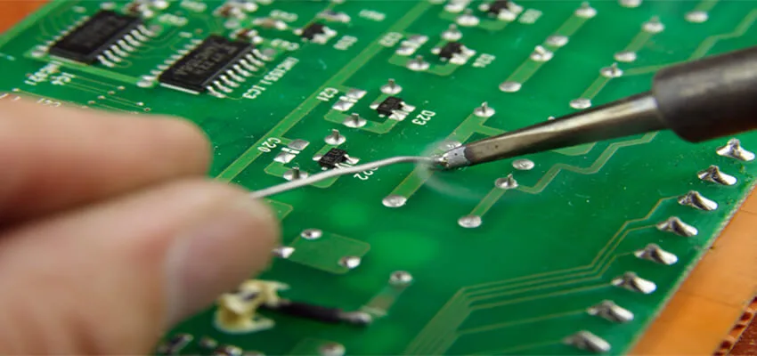
Wave Soldering
A technique of soldering components. The printed circuit board is passed through a liquified solder
heating system at a constant speed to generate a steady wave crest, and the solder wave crest will
solder the part pins and subjected pads together.
Surface Mount
A method of PCB assembly where the maker just needs to put digital elements on the circuit card and then
securely take care of the components on the pads via steps such as solder paste printing and reflow
soldering.
Reflow Soldering
melts the solder paste to attach the pads (SMD) and device pins.
Solder Bridging
Two connected pins on a part are connected, which is a printing mistake.
