PCB Prototyping Secrets Revealed in 13 Easy Steps

PCB Prototyping Can Be Done in the Following Way:
(1) Contact the factory: Inform the PCB factory of the size, the process requirements, the product quantity and any
other relevant information. Wait for the professionals to give you a PCB prototyping quote and then place your
order.
(2) Cutting: Based upon the engineering information supplied by the customer, make
small pieces from the large panels that meet the requirement.
(3) Drilling: Drill the holes that are required on the plate and the hole diameters at
the appropriate position.
(4) Copper Deposition: A thin copper layer is deposited using chemical methods on the
hole insulating.
(5) Graphic Transfer: Transfer the image from the production film onto the board.
(6) Graphic plating: Electroplating copper and gold-nickel, or tin layers of the
required thickness onto the copper foil exposed on the circuit pattern.
(7) Stripping: Remove the anti-plating film by using sodium hydroxide and alkaline
solution.
(8) Etching: Use chemical agents to remove noncircuit areas.
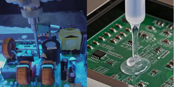
(9) The green ink: Apply the pattern from the film of the green ink to the board. This
is mainly done to protect the circuit, and to prevent tin forming when soldering the parts.
(10) Characters: Some characters have been printed on the circuit boards for easy
identification.

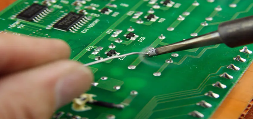
(11) Gold-plated fingers: The plug
fingers are plated with a nickel-or-gold layer to increase their durability and wear resistance.
(12) Forming: Cut out the desired shape using a CNC machine or a mold stamping.
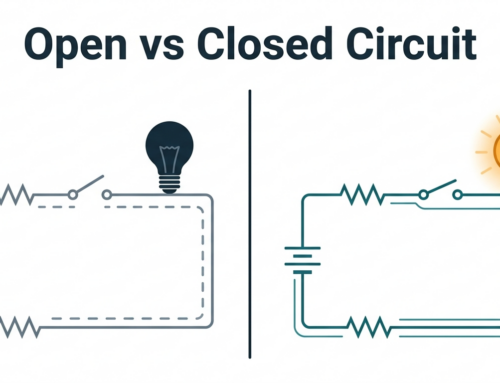
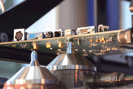
(13) Test: Use a flying probe to detect defects which affect functionality such as
short circuits or open circuits that are not readily visible.
Summary
PCB prototype plays a major role in the
development of electronic products. circuit prototyping allows us to verify the correctness of the
circuit design and evaluate product performance.
Circuit board prototyping has a direct impact on the quality of electronic devices. To ensure quality,
it is important to control each step of the PCB prototyping process.
