Understanding the Causes, Hazards, and Solutions for Circuit Board Warping and Bending

It is not surprising that the most common false is the bowing of printed circuit boards. Most new inspectors think that having a rigid, perfectly
flat board as a standard is a fallacy. Understanding the reasons and causes for PCB twist and bow during
the PCB Design phase can help resolve the issue.
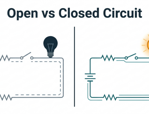
What Is the Difference Between Bow and Twist?
Let’s first discuss the differences between bow and twist. The board will lift off the panel if it
has a bow issue, even if all four corners of the board are in contact. (Think of the shape and form of a
bowed blade).

When three PCB corner are in contact and the fourth corner has been raised, warp can occur. IPC states
that both bend and warp must be evaluated to determine if the level of the warp or bend is acceptable.
Why Is It That the IPC Allows Bend or Warp to Be Allowed?
This is because of the materials and manufacturing processes used to make printed circuit boards. The
PCB laminates consist of epoxy resin and fiberglass cloth, each with its own thermal expansion
characteristics. If you add a copper layer to the PCB, either on one side or both sides, then you will
need to take into account additional thermal properties.
There is no guarantee of a uniform response across samples when the board manufacturer subjects the
material to different etching or heat treatment processes.
IPC allows tolerances because reactions can vary between samples, despite the strict manufacturing
process that PCB lamination manufacturers use for all laminates. The finished product should fall within
tolerances or parameters rather than exact numbers to account for normal variations. These tolerances
are set to allow smaller bend warps without affecting performance.
Bow and Twist: Other Effects
Bow and twist can be affected by other factors during board manufacture, such as:
• Additional Part Number Features
• Increased board layer count (additional material = additional heat treatment).
• Material mix (i.e. using a standard FR4 with a high-frequency laminate to control impedance, resulting
in stacked unbalanced)
Mix of Copper Weights
Copper has a large coefficient of thermal contraction, which can cause the bow to twist and break.
Copper with a higher density will expand more forcefully toward areas of minimal resistance than copper
with a lower density.
In a balanced stack, the thermal expansion values are opposite and opposing each other. This helps to
maintain an even bow force. Unbalancing the stack will cause one side to have a higher thermal expansion
value, which will then affect the entire board. Copper planes that are solid will expand differently
from signal layers, particularly if there is a lower signal density. All planes and signals should be on
the same side of the board.
PCB manufacturers must also ensure that laminates unprocessed are stored properly to keep them flat.
They should also be responsible for the ongoing work in order to avoid awkward stacking of panels.
Customers can be advised to steal copper if the design is prone bending or flexing.
Board Warping and Bending: Countermeasures
How can we avoid the board bending or warping as it passes through the reflow-oven?
1. Reduced temperature reduces stress on board
The main cause of board warping is “temperature”. By reducing the temperature in the
reflow-oven or slowing down the rate at which the board heats and cools, it is possible to reduce the
warping of boards. There may also be side effects.
2. Use high-Tg Boards
Tg stands for the glass transition temperature. This is the temperature where the material switches from
a glass to a rubber state. The lower the Tg of the material is, the quicker the board softens after
entering the reflow-oven. It will also take longer for the board to reach a rubbery state. A higher Tg
can improve the board’s ability to resist stress and deformation. However, the material costs more.
3. Increase the Thickness on the Circuit Board
Many electronic products have been thinned to 1.0mm or 0.8mm. With such a thick board, it is hard to
prevent the board from deforming as it passes through the reflow oven. If there is no requirement to be
thin, it is recommended that the board is 1.6mm thick. This will reduce the chance of the board
deforming and bending.
4. Reduce the Size and Number of Panels on the Circuit Board
Due to the fact that most reflow ovens drive the board forward using chains, the heavier the board is,
the more likely the board will be deformed and dented in the reflow. Try to place the long side of your
circuit board on the chain in the reflow oven. This will reduce denting and deformation due to the
weight. This is why fewer panels are used. To achieve the least dent deformation, it is best to pass
through the furnace using the narrow side that is perpendicular the furnace direction.
5. Use a Reflow Jig
The last resort, if the above methods fail to work, is to use a Reflow Pallet (reflow carrier/template).
This will reduce the deformation. Reflow pallets can be used to reduce board warping and bending. This
is because, regardless of whether it’s thermal expansion or contraction that is occurring, the
pallet is designed to fix the board until it reaches a temperature below the Tg and hardens again.
Conclusion
Orinew Technology Processing: PCB twisting and bending is a key factor in determining acceptable standards.
It also provides us with the parameters to prevent this from happening. The manufacturers need to know
the causes of printed-circuit board bending but cannot eliminate them. A better understanding will lead
to a more efficient and effective circuit board manufacturing and design process.
