What Are the Benefits of Using Blind Vias and Buried Vias on PCBs?

PCBs are often crowded and it can be difficult
to connect the components required to both sides of a board. Blind and buried vias are often the most
effective way to fit all of the necessary elements on the PCB. Many people don’t know what blind and
hidden vias are, or how to use these. Understanding what blind and buried vias are, and how they work is
important.
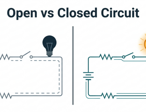
What Does a Via Mean?
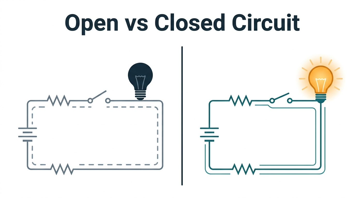
A via is a hole that has been drilled into the PCB or plated on it to allow signals to pass through to
the inner layer or other side. Vias are used to connect components that have planes or signals traces.
They allow changes to signal layers. Through-holes are usually used when a visa completely penetrates
the PCB. Some people may refer to this as a “through-hole”.
Blind and buried vias can only be used on boards that have at least four layers. They connect the inner
layers with other inner layers adjacent or next to them, as well as to the surface layer.

A Closer View of Blind Vias
When examining blind and hidden vias, there are many different types to consider. There are several
types of blind vias: photo-defined, controlled depth, sequential lamination, and laser-drilled.
Photo-defined blinds vias. Laminating photosensitive resin on a core is required to create a blind that
can be photo-defined. The photosensitive paper has a pattern which indicates where the hole should be
made. The remaining material is hardened by exposing the paper to light. The PCB then is placed in an
etching liquid that removes the material from the hole. The copper is then plated into the hole, and
also on the surface of the PCB.
Controlled Depth Blind Vias. Creating controlled depth blind through-holes is similar to creating
through-holes. The only difference between the two is that the drill is only set to penetrate a portion
of the PCB. The modern technology allows this to be done precisely, so that the features under the hold
don’t come in contact with the bit. The copper is then plated over the hole after it has been
drilled. It is the least expensive option but the hole must be large enough for a drill to machine. This
is a good solution for many PCBs, but it’s not the best option for everyone.
Lamination Sequential Blind Vias. Lamination Sequential blind vias can be made with a thin laminate
sheet. This process is similar in that the laminate is drilled and then plated before being etched. This
method creates the elements that will make up the second layer on the board. The copper sheet on the
other side will be the first layer. The component is laminated to additional layers before the final
steps of creating a PCB are completed. This method is not used anymore because it’s expensive.
Laser Drilled Vias. Laser-drilled blind throughs are created after the PCB has been laminated, but
before the outer layers have been etched and laminated. There are many different types of lasers that
can be used today to create the holes. However, the results are always the same.
A Closer View of Buried Vias
A buried via is a via that passes between two layers on a PCB, but doesn’t touch either surface. A
buried via creates a link between two internal layers. The via is “buried”, as the name
suggests, within the PCB. A buried via has a similar purpose to a blind via in that it is used to ensure
the PCB is equipped with all of the necessary features. Buried vias can help you free up space on your
board. You can create buried vias by creating an inner layer of vias and then adding additional layers
on the outside.
The Benefits of Blind and Buried Vias
Blind and buried vias are a great way to save space on PCBs. You can reduce the size of your PCB. This
is important when working with electronic components. Vias allow you to free up space on your
board’s surface. This space can be used for additional features. Vias may seem like a simple
solution. However, adding buried and blind vias to your board can raise the price.
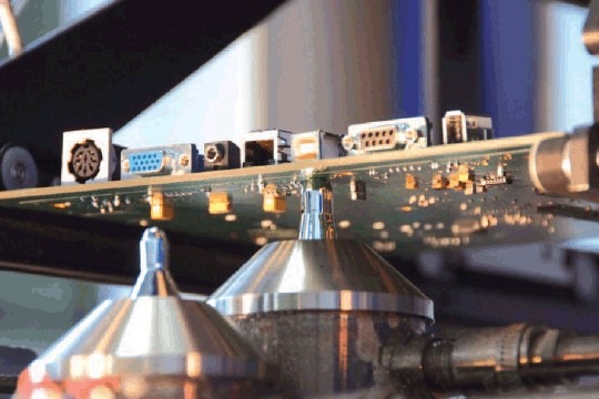
It’s crucial to work with an experienced manufacturer because there are many factors involved in
getting the correct PCB with blind and buried throughs.
How to Choose the Right PCB Manufacturer For Blind and Buried Vias
It is best to leave the delicate task of adding blind or buried vias on your PCB to a professional
manufacturer. Finding the right manufacturer is therefore more important. Orinew Technology is a PCB manufacturer
that has been around for 15 years. We offer a variety of services and technologies designed to make your
life easier. We can design simple or complex boards depending on your requirements.
Working with us has many advantages. We provide 24/7 support, and we deliver quickly. You can also get
an instant online quote for SMT patches. This will give you a good idea of the cost of your project and
how to track it. Contact Orinew Technology’s SMT
manufacturers if you have questions about blind or buried vias.
