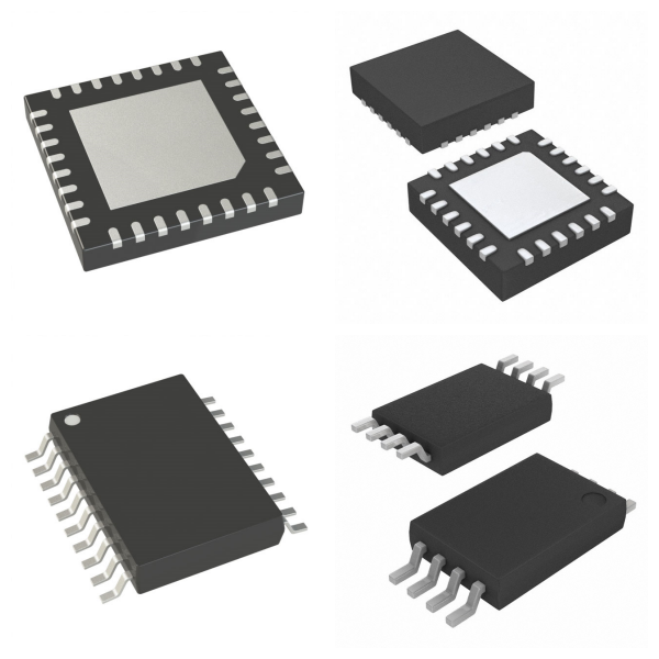
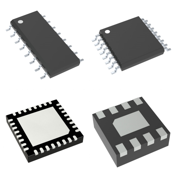
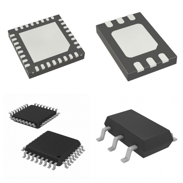
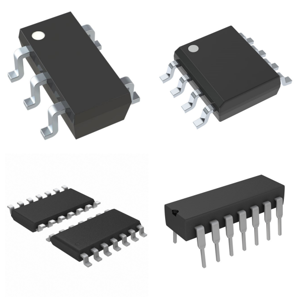
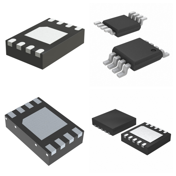
New title

<h1> Application Specific Clock/Timing </h1> <p> Application Specific Clock ICs (ASCIs) are electronic devices that provide clock signals for specific applications. Unlike RTCs, which have real-time clock calendars and operate independently of a host device, ASCIs are designed to meet the timing requirements of a particular application. </p> <p>   </p> <p> ASCIs are used in a wide range of applications, including data communication, networking, and digital signal processing. They provide the necessary clock signals to synchronize data transfer between devices, ensure the accurate timing of data transmissions, and enable efficient processing of data signals. </p> <p>   </p> <h3> <strong>Some common types of ASCIs include:</strong> </h3> <p> <strong>Ethernet PHY Clocks:</strong> These ICs provide the clock signals needed by Ethernet Physical Layer (PHY) transceivers to transmit and receive data on an Ethernet network. </p> <p> <strong>PCI Express Clocks:</strong> These ICs provide the clock signals required by PCI Express devices to ensure reliable data transmission and reception. </p> <p> <strong>Audio Clocks:</strong> These ICs generate clock signals for audio applications such as digital audio interfaces, audio codecs, and digital signal processors. </p> <p> <strong>Video Clocks:</strong> These ICs generate clock signals for video applications such as video codecs, display controllers, and digital video recorders. </p> <p>   </p> <p> ASCIs are critical components for many modern electronic systems. They provide the precise timing signals needed for reliable data transfer, processing, and synchronization in a wide range of applications. </p> <p>
<h1> Clock Buffers, Drivers </h1> <h2> 1. What are the Basic Functions of Clock Buffers, Drivers? </h2> <p> <strong>‌Signal Fan-out and Drive Enhancement</strong>‌ </p> <p> The clock buffer replicates a single input clock signal into multiple outputs through a non-PLL structure, providing fan-out capability to meet the system's multi-component synchronization requirements, while strengthening signal drive capabilities to reduce distortion. For example, Renesas' clock buffer supports output frequencies up to 3.2GHz and covers signal types such as LVCMOS and LVDS. </p> <p>   </p> <p> <strong>‌Format and Level Conversion</strong>‌ </p> <p> Supports conversion of different signal formats (such as LVPECL to LVDS) and level standards to adapt to diverse circuit design requirements. Some devices also support mixed output modes for flexible configuration. </p> <h2>   </h2> <h2> 2. What are the Key Parameters of Clock Buffers, Drivers? </h2> <h3> 1) ‌Performance Parameters‌ </h3> <p> ‌<strong>Number of Output Channels‌</strong>: Mainstream products can provide 5-27 output channels to meet the needs of high-density systems; </p> <p>   </p> <p> <strong>‌Jitter and Phase Noise‌</strong>: The jitter added by the buffer itself will be superimposed on the original clock source, directly affecting the timing margin of the high-speed system, and its additional jitter value (such as 50fs level) needs to be paid attention to; </p> <p> <strong>‌Transmission Delay‌</strong>: Determined by the load resistance and output capacitance, the delay can be reduced by optimizing the tail current and slew rate. </p> <p>   </p> <h3> 2) ‌Electrical Characteristics‌ </h3> <p> <strong>‌Power Consumption and Voltage‌</strong>: Support 1.2V to 3.3V power supply, low power design reduces system energy consumption; </p> <p> <strong>‌Duty Cycle Stability‌</strong>: Directly affects the symmetry of the clock signal, and the output duty cycle error must be less than ±2%. </p> <p>   </p> <h2> 3. What are Clock Buffers, Drivers Used for? </h2> <p> <strong>‌High-speed Communication System</strong>‌ </p> <p> Used in 5G base stations, data centers, and other scenarios, the timing accuracy of high-speed interfaces (such as PCIe and Ethernet) is guaranteed by reducing jitter and noise. </p> <p>   </p> <p> <strong>‌Multi-chip Synchronization</strong>‌ </p> <p> Use a single master clock source with a buffer instead of a multi-crystal oscillator solution to reduce costs and solve synchronization problems. </p> <p>   </p> <h2> 4. What is the Typical Structure of Clock Buffers, Drivers? </h2> <p> <strong>‌Buffer Circuit Design</strong>‌ </p> <p> Usually, an even-numbered inverter cascade structure is used, and the driver size is gradually increased to balance power consumption and delay, and optimize the driver ratio (such as 2.718:1). </p> <p>   </p> <p> <strong>‌Zero Delay Buffer</strong>‌ </p> <p> PLL is integrated into the special design to eliminate the phase difference between input and output, which is suitable for scenarios sensitive to delay. </p> <p>   </p> <h2> 5. Clock Buffers, Drivers FAQs </h2> <h3> 1) What is the core function of the ‌Clock Buffer? ‌ </h3> <p> It is mainly used to copy a single clock signal into multiple outputs (fan-out), support format conversion (such as differential to single-ended), level conversion, and reduce the risk of distortion during long-distance signal transmission. </p> <p>   </p> <p> Some models (such as zero delay buffers) achieve input and output clock phase alignment through internal feedback loops to reduce timing deviation. </p> <p>   </p> <h3> 2) How to classify ‌Clock Buffer‌? ‌ </h3> <p> ‌<strong>Fan-out Buffer‌</strong>: simply copy the clock signal, typical applications such as Renesas Electronics' LVCMOS buffer, support more than 10 fan-outs. </p> <p>   </p> <p> <strong>‌Zero Delay Buffer‌</strong>: Synchronizes input and output clock phases through PLL, suitable for scenarios with strict timing requirements. </p> <p>   </p> <h3> 3) ‌Which parameters affect system timing? ‌ </h3> <p> <strong>‌Output-to-Output Skew‌</strong>: The maximum time difference between multiple output clocks, which directly affects the timing margin of high-speed interfaces (such as setup/hold time). </p> <p> <strong>‌Additive Jitter‌</strong>: The jitter introduced by the buffer itself, superimposed on the clock source jitter, the formula is total jitter = √(source jitter² + additive jitter²). </p> <p> <strong>‌Drive Capability‌</strong>: The number of loads and wiring length must match the fan-out capability of the buffer. </p> <p>   </p> <h3> 4) ‌How to quantify the impact of additive jitter? ‌ </h3> <p> If the clock source jitter is 300fs, adding a 50fs buffer only increases the total jitter to 304fs; but when the source jitter drops to 50fs, the total jitter will deteriorate to 70.7fs3. </p> <p>   </p> <h3> 5) ‌Which indicators should be paid attention to when selecting? ‌ </h3> <p> <strong>‌Input Type‌</strong>: Supports flexibility of interfaces such as LVDS, HCSL, and LVCMOS. </p> <p> <strong>‌Output Quantity and Format‌</strong>: Select the single-ended/differential output ratio according to the system load requirements. </p> <p> <strong>‌Power Consumption and Temperature Range‌</strong>: Wide temperature and low power consumption models should be preferred for high-temperature or high-density scenarios. </p> <p>   </p> <h3> 6) ‌How to reduce timing deviation? ‌ </h3> <p> Prefer buffers with output skew <50ps, and reduce PCB trace differences through symmetrical layout. </p> <p>   </p> <p> In FPGA development, combine the DONT_TOUCH attribute to retain the key buffer layout. </p> <p>   </p> <h3> 7) ‌How to handle multi-clock domain synchronization? ‌ </h3> <p> Zero delay buffers lock the input clock phase through internal PLL to avoid cross-clock domain data conflicts. </p> <p>
<h1> Clock Generators, PLLs, Frequency Synthesizers </h1> <h2> 1. What are Phase-Locked Loops (PLLs)? </h2> <h3> 1) Definition and Structure </h3> <p> PLL is a feedback control system that dynamically adjusts the output frequency and phase of the voltage-controlled oscillator (VCO) by comparing the phase difference between the input reference signal and the feedback signal, and finally achieves signal synchronization. Its core components include a phase comparator, loop filter, VCO, and divider. </p> <p>   </p> <h3> 2) ‌Core Functions‌ </h3> <p> <strong>Frequency Synthesis and Tracking</strong>: Generate stable high-frequency signals and maintain phase lock with the input reference signal. </p> <p> <strong>Noise Suppression</strong>: Reduce phase jitter and noise interference through loop filters. </p> <p>   </p> <h3> 3) ‌Typical Applications‌ </h3> <p> <strong>Communication Systems</strong>: used for the local oscillator (LO) signal generation, FM demodulation, and carrier recovery. </p> <p> <strong>Digital Circuits</strong>: Provide low-jitter clock signals for FPGAs and processors. </p> <p>   </p> <h2> 2. What are Clock Generators? </h2> <h3> 1) Definition and Composition‌ </h3> <p> The clock generator works together with the oscillator (OSC) and PLL to generate the main clock signal required by the system. The OSC provides a low-frequency reference clock, and the PLL multiplies it to a high frequency. </p> <p>   </p> <h3> 2) ‌Key Technical Features‌ </h3> <p> <strong>Low Phase Noise</strong>: ensures the stability of timing circuits. </p> <p> <strong>Programmability</strong>: supports dynamic adjustment of output frequency (such as flexible configuration in FPGA). </p> <p>   </p> <h3> 3) ‌Application Scenarios‌ </h3> <p> <strong>Microprocessors and memories</strong>: provide synchronous clocks for internal modules of the chip. </p> <p> <strong>Communication interfaces</strong>: clock management for high-speed data transmission such as PCIe and USB. </p> <p>   </p> <h2> 3. What are Frequency Synthesizers? </h2> <p>   </p> <h3> 1) Implementation Method‌ </h3> <p> Frequency synthesizers generate high-precision, wide-range frequency signals through phase-locked loops (PLLs), direct digital synthesis (DDS) or hybrid architectures. Typical structures such as charge pump phase-locked loops (CPPLLs) include modules such as frequency detectors (PFDs), charge pumps (CPs), and VCOs. </p> <p>   </p> <h3> 2) ‌Core Advantages‌ </h3> <p> <strong>High-frequency Output</strong>: suitable for high-bandwidth scenarios such as millimeter-wave communications. </p> <p> <strong>Fast Frequency Switching</strong>: meets the needs of multi-band switching in wireless communications. </p> <p>   </p> <h3> 3) ‌Typical Applications‌ </h3> <p> <strong>RF Transceiver Systems</strong>: provide local oscillator signals for 5G and satellite navigation. </p> <p> <strong>Radar and Test Equipment</strong>: generate highly stable modulation waveforms. </p> <p>   </p> <h2> 4. Relationship and Collaborative Application of the Three </h2> <p> <strong>‌Hierarchical Dependency‌</strong>: The clock generator is often used as a basic module to provide a reference clock; PLL is used for frequency multiplication and synchronization; the frequency synthesizer further expands the output frequency range. </p> <p>   </p> <p> ‌<strong>System Integration‌</strong>: In modern SoCs and FPGAs, the three are often integrated to achieve a flexible clock network to meet the diverse needs of communication, computing, and storage. </p> <p>   </p> <p> <strong>‌Performance Indicators‌</strong>: Phase noise, lock time and power consumption need to be paid attention to, especially in portable devices, energy efficiency needs to be optimized. </p> <p>   </p> <p> Through the cooperation of the above modules, electronic systems can achieve high-precision timing control, multi-band compatibility, and anti-interference capabilities, supporting complex applications in the fields of communication, computing, and embedded systems. </p> <p>
<h1> Delay Lines </h1> <p> Delay line ICs are a type of electronic components used to precisely control signal delay time. They mainly achieve time delay by regulating the transmission path of electrical or optical signals, and continue to play a core role in high-speed electronic systems, optical communications, and precision measurement. </p> <p>   </p> <h2> 1. How do Delay Lines Work?‌ </h2> <p> Delay line ICs achieve delay control based on the difference in signal propagation time in the medium. Digital types achieve programmable delays through digital circuits such as shift registers and FPGAs, while analog types use transmission line characteristics or dedicated semiconductor processes to achieve nanosecond precision adjustment. Some high-end products combine voice coil motor drive technology to support microsecond response speed and picosecond precision. </p> <p>   </p> <h2> 2. What are the ‌Main Types of Delay Lines?‌ </h2> <p> <strong>‌Programmable Delay Line‌</strong>: such as Dallas Semiconductor's DS1020/1021 series, which supports serial/parallel interface programming, with a delay range of 10ns to 520ns and adjustable step size (0.15ns to 5ns). </p> <p>   </p> <p> ‌<strong>Fixed Delay Line‌</strong>: Suitable for fixed delay requirements in specific scenarios, such as synchronization signal calibration. </p> <p>   </p> <p> <strong>‌Multifunctional Delay Line‌</strong>: For example, DS1023 supports signal inversion and pulse width modulation, which expands the application scenarios. </p> <p>   </p> <h2> 3. What are the ‌Technical Advantages of Delay Lines?‌ </h2> <p> <strong>‌High Precision‌</strong>: Closed-loop control technology can achieve femtosecond delay adjustment. </p> <p> <strong>‌Fast Response‌</strong>: The response time of the fiber delay line driven by the voice coil motor reaches the microsecond level. </p> <p> <strong>‌Integration‌</strong>: The silicon-based optical delay line adopts a microring resonator cascade structure, supports 11-bit delay adjustment, and is easy to integrate into the system. </p> <p>   </p> <h2> 4. What are Delay Lines Used for?‌ </h2> <p> <strong>‌Communication System‌</strong>: Compensate for signal transmission time difference and improve synchronization performance. </p> <p> <strong>‌Radar and Measurement‌</strong>: Target distance detection is achieved through time delay. </p> <p> <strong>‌Digital Signal Processing‌</strong>: Used in scenarios such as clock alignment and anti-aliasing filtering. </p> <p>   </p> <h2> 5. ‌Representative Products for Delay Lines‌ </h2> <p> Dallas Semiconductor's DS series (such as DS1045 dual delay line) and Thorlabs' fiber delay line ODL series are industry benchmark products, among which DS1045 provides dual-channel independent control function with a delay range of 9ns to 84ns. </p> <p>   </p> <h2> 6. ‌Development Trend of Delay Lines‌ </h2> <p> With the growing demand for optical communications and high-speed computing, silicon-based optical delay lines with high integration and wide adjustment range (picoseconds to nanoseconds) have gradually become mainstream, combining electro-optical/thermo-optical effects to achieve fast and stable adjustment. </p> <p>   </p> <h2> 7. Delay Lines FAQs </h2> <h3> 1) ‌Why does a delay line cause signal reflection? ‌ </h3> <p> The impedance mutation of the transmission line in the delay line will cause signal reflection. The transmission line impedance can be made continuous by adding termination matching resistors (such as 50Ω and 75Ω). Refer to the termination technology in signal integrity processing. </p> <p>   </p> <h3> 2) ‌How to evaluate the impact of delay lines on timing? ‌ </h3> <p> It is necessary to combine the setup time (Setup Time) and hold time (Hold Time) indicators to ensure that the signal meets the stability window requirements before and after the clock edge. If necessary, the risk of metastability can be eliminated through synchronization logic. </p> <p>   </p> <h3> 3) ‌How to choose a delay scheme when transmitting across clock domains? ‌ </h3> <p> For single-bit signal transmission, a 2-level trigger synchronizer can be used for low-speed to high-speed scenarios, and a handshake protocol or asynchronous FIFO is required for high-speed to low-speed scenarios; Gray-coded asynchronous FIFO is recommended for multi-bit signals. </p> <p>   </p> <h3> 4) ‌What problems will the delay line delay accuracy cause? ‌ </h3> <p> It may cause synchronization failure or metastability, and the timing margin of different clock domains needs to be verified through timing constraint analysis (input_delay/output_delay). </p> <p>   </p> <h3> 5) ‌How to optimize the wiring layout of the delay line IC? ‌ </h3> <p> Use differential pair equal-length wiring to reduce the transmission delay difference </p> <p> Increase the spacing between high-speed signals and sensitive signals (such as the 3W rule) </p> <p> Prioritize the use of inner layer routing to reduce radiation interference. </p> <p>   </p> <h3> 6) ‌How to ensure the electromagnetic compatibility of the delay line IC? ‌ </h3> <p> It is necessary to meet EMC standards such as EN 55032 and reduce high-frequency radiation interference through reasonable grounding design, power decoupling capacitor configuration, and shielding structure. </p> <p>   </p> <h3> 7) ‌How to detect metastability caused by delay lines? ‌ </h3> <p> Check the recovery time constraints of the trigger through formal verification tools. The synchronous circuit needs to meet: the first-level metastable recovery time + the second-level setup time ≤ the clock cycle. </p> <p>
<h1> IC Batteries </h1> <h2> 1. What are IC Batteries? </h2> <p> IC batteries, also known as integrated circuit batteries or micro batteries, are small batteries integrated into microchips or integrated circuits to provide a stable power supply to ICs in the absence of an external power source to maintain their functions. </p> <p>   </p> <h2> 2. What are the Types of IC Batteries? </h2> <p> IC batteries are divided into rechargeable batteries and non-rechargeable batteries. Rechargeable IC batteries can be charged using an external power source, while non-rechargeable IC batteries are designed to have a fixed service life and need to be replaced afterwards. </p> <p>   </p> <h2> 3. What are the Materials of IC Batteries? </h2> <p> IC batteries can be made of a variety of materials, including lithium, silver oxide, and zinc-air batteries. They are usually less than 1 mm in size and have a lower capacity compared to standard batteries. However, they are designed to operate for a long time with extremely low power consumption, which is very suitable for applications that require low power consumption and long-term autonomous operation, such as medical implants, RFID tags, and sensors. </p> <p>   </p> <h2> 4. Collaborative Application of Batteries and ICs </h2> <h3> 1) ‌Battery Basic Structure‌ </h3> <p> It is composed of a cathode (reduction reaction), an anode (oxidation reaction), an electrolyte (ion transport medium), a separator (preventing short circuits), and a collector (current collection). Types include lithium-ion, nickel-hydrogen batteries, etc. </p> <p>   </p> <p> Cells are connected in series or in parallel to form battery packs and finally integrated with BMS and other modules to form a complete battery pack. </p> <p>   </p> <h3> 2) ‌Role of IC in Battery System‌ </h3> <p> <strong>‌Energy Management‌</strong>: Charging and discharging control, temperature monitoring, and overvoltage protection are achieved through dedicated ICs, such as power management chips (PMIC) to optimize energy efficiency. </p> <p> <strong>‌Communication and Control‌</strong>: Microcontrollers (MCU) or sensor interface ICs are used to ensure data transmission and balanced control between battery packs. </p> <p>   </p> <h3> 3) ‌Typical Cases‌ </h3> <p> <strong>‌Mobile Devices‌</strong>: High-density BGA packaged ICs are used in combination with lithium polymer batteries to achieve a lightweight design. </p> <p> <strong>‌Energy Storage System‌</strong>: Multi-cell battery packs achieve remote monitoring and fault diagnosis through CAN bus communication ICs. </p> <p>
<h1> Programmable Timers and Oscillators </h1> <h2> 1. What are Programmable Timers and Oscillators?‌ </h2> <p> <strong>‌Programmable Timer‌</strong>: Controls time delay or oscillation frequency through external resistor and capacitor networks, supports monostable (fixed delay) and astable (continuous oscillation) modes, typical applications such as SA555DR can achieve timing range from microseconds to hours, and output TTL compatible signals. </p> <p> <strong>‌Programmable Oscillator‌</strong>: Generates precise frequency signals based on crystal or MEMS technology. For example, the frequency of a quartz crystal oscillator is determined by the physical properties of the crystal, and the load capacitor needs to be used to adjust the accuracy; MEMS oscillators (such as SiTime products) adjust the frequency through programming and have stronger anti-electromagnetic interference (EMI) capabilities. </p> <p>   </p> <h2> 2. What are Programmable Timers and Oscillators Used for?‌ </h2> <p> <strong>‌Industrial Control‌</strong>: High-precision timing chips (such as EH4B03) are used in scenarios such as equipment timing control and sensor data acquisition, and support harsh environments (-40°C to 85°C). </p> <p> <strong>‌Communication System‌</strong>: In scenarios where high-stability clock synchronization is required (such as serial communication), crystal oscillators can reduce data errors. </p> <p>   </p> <p> <strong>‌Consumer Electronics‌</strong>: A 555 timer is used for simple control functions such as PWM dimming and buzzer driving. </p> <p>   </p> <h2> 3. ‌Key Considerations for Selecting Programmable Timers and Oscillators‌ </h2> <p> <strong>‌Performance Requirements‌</strong>: </p> <p> Select crystal oscillators (such as 12MHz quartz crystals) when timing accuracy is high; </p> <p>   </p> <p> MEMS oscillators (such as SiTime products) are preferred for anti-interference scenarios. </p> <p>   </p> <p> <strong>‌Cost and Supply Chain‌</strong>: </p> <p> For general needs, mature models (such as SA555DR) can be selected, and attention should be paid to inventory and price fluctuations; </p> <p>   </p> <p> For special frequency or packaging needs, the supply cycle and alternative solutions need to be evaluated. </p> <p>   </p> <h2> 4. ‌Common Problems and Solutions for Programmable Timers and Oscillators‌ </h2> <p> <strong>‌Timing Deviation‌</strong>: Check whether the external RC network parameters match or whether the load capacitance is calibrated (common problems with crystal oscillators). </p> <p> <strong>‌Output Instability‌</strong>: Check for power supply noise or EMI interference, and replace with an anti-interference oscillator if necessary. </p> <p> <strong>‌Package Compatibility‌</strong>: Small package chips such as SOT23-6 (such as EH4B03) need to pay attention to heat dissipation and welding processes. </p> <p>   </p> <h2> 5. ‌Replacement and Compatibility of Programmable Timers and Oscillators‌ </h2> <p> Some MEMS oscillators (such as the SiTime SE series) can directly replace traditional quartz oscillators, but the frequency tolerance and drive capability need to be re-evaluated. </p> <p>   </p> <p> Timer chips (such as the 555 series) have similar functions, but the pin definitions may be different. When replacing, refer to the datasheet. </p> <p>
<h1> Real Time Clocks </h1> <p> RTC (Real-Time Clock) is a timing device used to accurately track date and time, and can run independently of the main system. Its core feature is that it relies on a backup power supply (such as a button battery) to keep timing when the main power is disconnected, and communicates with the main system through interfaces such as I²C and SPI. </p> <p>   </p> <h2> 1. What are the Core Functions of Real Time Clocks? </h2> <p> <strong>‌Accurate Time Keeping‌</strong>: Independently provide calendar time information such as year, month, day, hour, minute, and second, and continue to run through a backup battery after the main power of the system is turned off to ensure uninterrupted time. </p> <p> <strong>‌Low Power Design‌</strong>: Compared with the clock module integrated into the microcontroller (MCU), the independent RTC can significantly reduce system power consumption and avoid frequent waking up of the MCU. </p> <p>   </p> <h2> 2. Hardware Composition of Real Time Clocks </h2> <p> <strong>‌Core Components‌</strong>: Contains a crystal oscillator (usually a 32.768kHz crystal), a clock chip, and a backup battery. </p> <p> <strong>‌Oscillation Principle‌</strong>: The 32.768kHz crystal oscillator generates an accurate 1Hz clock signal after 15 frequency divisions (2^15=32768), which is the basis for timing. </p> <p> <strong>‌Temperature Compensation‌</strong>: Built-in temperature sensor and compensation algorithm offset the frequency drift of the crystal oscillator caused by ambient temperature changes, and improve the accuracy of the entire temperature range (such as ±3.5ppm). </p> <p>   </p> <h2> 3. Key Features of Real Time Clocks </h2> <p> <strong>‌Register Architecture‌</strong>: 32-bit counter stores BCD format time data, supports leap year, month day automatic correction. </p> <p>   </p> <p> Provides sub-second binary counter to meet high-precision timing requirements. </p> <p>   </p> <p> <strong>‌Interface and Control‌</strong>: Supports serial interfaces such as I²C, SPI, and 3-Wire to reduce pin occupancy. </p> <p>   </p> <p> Programmable prescaler, alarm interrupt, and timed wake-up function. </p> <p>   </p> <p> <strong>‌Power Redundancy‌</strong>: The main power supply and backup battery automatically switch to ensure continuous operation after power failure. </p> <p>   </p> <h2> 4. What are Real Time Clocks Used for? </h2> <p> <strong>‌Smart Meter‌</strong>: The core timing unit for remote meter reading and time-of-use electricity price billing, which must meet the requirements of wide temperature range, long life, and high precision. </p> <p> <strong>‌Embedded System‌</strong>: The time base of industrial control and communication equipment, used for event recording and timing task triggering. </p> <p> <strong>‌Consumer Electronics‌</strong>: Calendar and alarm functions of mobile phones, smartwatches, and other devices. </p> <p>   </p> <h2> 5. Typical Manufacturers and Products of Real Time Clocks </h2> <p> <strong>‌Maxim/TI/NXP‌</strong>: Provide full-featured RTC chips, support temperature compensation, and multiple interface options. </p> <p> <strong>‌Diodes‌</strong>: Launch RTC modules with integrated crystal oscillators (such as RT3A3241N3) to simplify design and improve reliability. </p> <p>   </p> <h2> 6. Technical Advantages of Real Time Clocks </h2> <table> <tbody> <tr class="firstRow"> <td width="164" valign="top" style="padding: 0px 7px; border-width: 1px; border-color: windowtext; background: rgb(190, 190, 190);"> <p> ‌Features </p> </td> <td width="404" valign="top" style="padding: 0px 7px; border-width: 1px; border-color: windowtext; background: rgb(190, 190, 190);"> <p> Value Realization </p> </td> </tr> <tr> <td width="164" valign="top" style="padding: 0px 7px; border-left-width: 1px; border-left-color: windowtext; border-right-width: 1px; border-right-color: windowtext; border-top: none; border-bottom-width: 1px; border-bottom-color: windowtext;"> <p> ‌Independent Power Supply </p> </td> <td width="404" valign="top" style="padding: 0px 7px; border-left-width: 1px; border-left-color: windowtext; border-right-width: 1px; border-right-color: windowtext; border-top: none; border-bottom-width: 1px; border-bottom-color: windowtext;"> <p> Maintain Uninterrupted Timing after the Main System is Powered Off </p> </td> </tr> <tr> <td width="164" valign="top" style="padding: 0px 7px; border-left-width: 1px; border-left-color: windowtext; border-right-width: 1px; border-right-color: windowtext; border-top: none; border-bottom-width: 1px; border-bottom-color: windowtext;"> <p> ‌Ultra-low Power Consumption </p> </td> <td width="404" valign="top" style="padding: 0px 7px; border-left-width: 1px; border-left-color: windowtext; border-right-width: 1px; border-right-color: windowtext; border-top: none; border-bottom-width: 1px; border-bottom-color: windowtext;"> <p> Extend the Life of Battery-powered Equipment </p> </td> </tr> <tr> <td width="164" valign="top" style="padding: 0px 7px; border-left-width: 1px; border-left-color: windowtext; border-right-width: 1px; border-right-color: windowtext; border-top: none; border-bottom-width: 1px; border-bottom-color: windowtext;"> <p> ‌High-precision Compensation </p> </td> <td width="404" valign="top" style="padding: 0px 7px; border-left-width: 1px; border-left-color: windowtext; border-right-width: 1px; border-right-color: windowtext; border-top: none; border-bottom-width: 1px; border-bottom-color: windowtext;"> <p> Full Temperature Range Error ≤3.5ppm (such as -40℃~85℃) </p> </td> </tr> <tr> <td width="164" valign="top" style="padding: 0px 7px; border-left-width: 1px; border-left-color: windowtext; border-right-width: 1px; border-right-color: windowtext; border-top: none; border-bottom-width: 1px; border-bottom-color: windowtext;"> <p> ‌Modular Design </p> </td> <td width="404" valign="top" style="padding: 0px 7px; border-left-width: 1px; border-left-color: windowtext; border-right-width: 1px; border-right-color: windowtext; border-top: none; border-bottom-width: 1px; border-bottom-color: windowtext;"> <p> Integrated Crystal Oscillator Reduces Peripheral Circuits and Improves Anti-interference Ability </p> </td> </tr> </tbody> </table> <p>   </p> <p> The current mainstream RTC has developed into a highly integrated temperature compensation module, which maintains ppm-level accuracy in an environment of -40℃ to 85℃and has become a core timing solution in the fields of Internet of Things and energy metering. </p> <p> <br /> </p><strong></strong>

Clock/Timing

‌1. What are Clock and Timing ICs?‌

‌The Core Difference between Clock IC and Timing IC‌

Clock IC (such as RTC chip) is mainly used to output stable clock signal and provide synchronization reference for processors, communication equipment, etc. Its core function is to generate accurate frequency signals through crystal frequency division.


Timing IC focuses on generating programmable time intervals or delay signals, usually integrating oscillator and counter, suitable for automation control, timing switch, and other scenarios.


The Role of Crystal Oscillators in Two Types of IC‌

Both rely on crystal oscillators as oscillation sources. Clock IC mostly uses 32.768kHz crystal (error ≤±20ppm) because of its high-frequency stability and low power consumption; timing IC can choose crystal or RC oscillation mode according to demand, the latter is lower in cost but poorer in accuracy.


2. What are Clock and Timing ICs Used for?‌

1) ‌Clock IC‌

Synchronous Digital System: microcontroller, FPGA, and other occasions that require global clock synchronization.

Communication Equipment: timing control of the router, time synchronization of 5G base station.


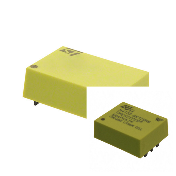
Consumer Electronics: mobile phone real-time clock (RTC), low-power timing of smart wearable devices.


2) ‌Timing IC‌

Industrial Control: Delay triggering of production line automation equipment, cyclic task management.

Home Appliances: LED flashing control, washing machine program timing.

Security System: sensor signal acquisition interval setting.


3. Common Faults and Solutions of Clock and Timing ICs‌

1) The ‌Crystal Oscillator does not Oscillate‌

‌Cause‌: PCB wiring is too long/interference (such as cross-wires between crystal pins), crystal oscillator quality defects, improper capacitor matching.

‌Countermeasures‌: Optimize routing (shorten the path, avoid parallel signal lines), replace high-precision crystal oscillators, and adjust ground capacitance parameters.


2) ‌Timing Error Accumulation‌

‌Cause‌: Crystal oscillator temperature drift (frequency is affected by temperature), power supply voltage fluctuations and aging effects.

‌Improvement‌: Use temperature-compensated crystal oscillators (TCXOs), add power supply filtering circuits, calibrate regularly, or select chips with automatic timing functions.


3) ‌Timing Function Failure‌

‌Hardware Problems‌: Short circuit caused by residual solder flux and abnormal chip power supply.

‌Troubleshooting Steps‌: Clean PCB solder joints, measure power supply voltage stability, and replace spare chips for verification.


‌4. Selection and Maintenance Recommendations for Clock and Timing ICs‌

1) ‌Key Selection Parameters‌

Clock IC: frequency stability (such as ±5ppm), power consumption (RTC often requires μA level), interface compatibility (I²C/SPI).

Timing IC: timing accuracy (error range), operating voltage range, output signal type (PWM/level).


2) ‌Long-term Maintenance Measures‌

Avoid drastic changes in ambient temperature and humidity to prevent crystal oscillator parameter drift.


Check the battery voltage (if any) regularly to prevent RTC data loss.


Use redundant design (such as dual crystal backup) to improve the fault tolerance of high-reliability systems.