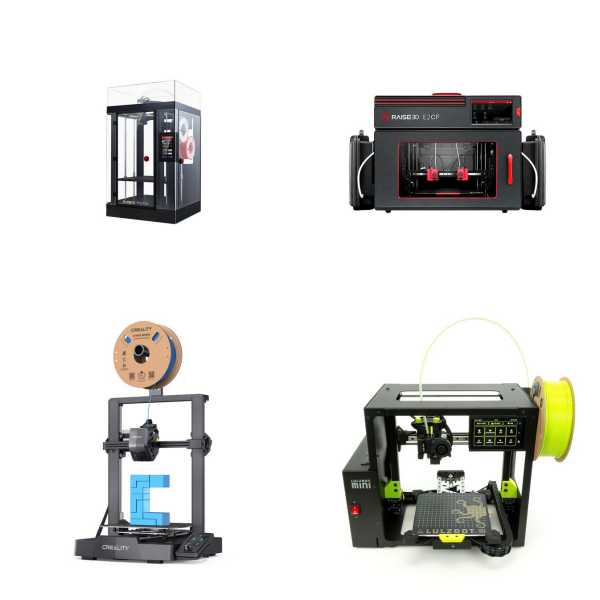
<h1> 3D Printers </h1> <p> A 3D printer (also known as a three-dimensional printer) is a computer-controlled device based on additive manufacturing technology that creates three-dimensional objects by layering materials (such as plastic, metal, or resin). This technology generates solid objects directly from computer graphics data, significantly different from traditional two-dimensional printing methods. </p> <p> </p> <p> In the field of electronic components, 3D printers have become a key tool for innovative manufacturing, particularly suitable for rapid prototyping and low-volume production. Its core applications include: </p> <p> </p> <p> PCB Manufacturing: By directly printing conductive materials (such as silver or copper-infused inks) or creating hollow grooves and then filling them with conductors, 3D printers enable rapid production of circuit boards, significantly shortening traditional PCB manufacturing cycles and supporting the design of complex three-dimensional structures. </p> <p> </p> <p> Flexible Electronics and Embedded Circuits: Using conductive copper paste technology, sensors, antennas, or heating elements can be printed on flexible substrates. These applications include wearable devices (such as smart clothing or medical patches), IoT devices, and automotive component integration, achieving structural and functional integration. </p> <p> </p> <p> In addition, 3D printing supports on-demand personalization and high-frequency radio frequency applications (such as 5G antenna manufacturing), reducing inventory costs and improving production efficiency. </p> <p> </p> <p> Future development will focus on improving precision and multi-material compatibility, promoting the popularization of consumer and industrial-grade equipment in scenarios such as electronic prototype repair and customized production. </p>
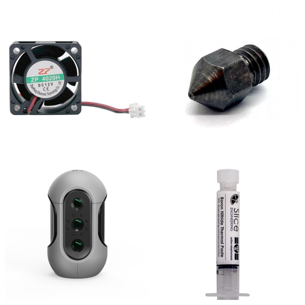
<h1> 3D Printing Accessories </h1> <p> 3D printing accessories enhance your printing experience by providing advanced features not typically included with base level 3D printers. Typical upgrades include build sheets and platforms, heaters, extruders, enclosures, and heads. Whether you are looking for a build sheet to securely hold an object or an advanced extruder head to 3D print objects with tight tolerances, we have upgrades for your 3D printing setup. </p>
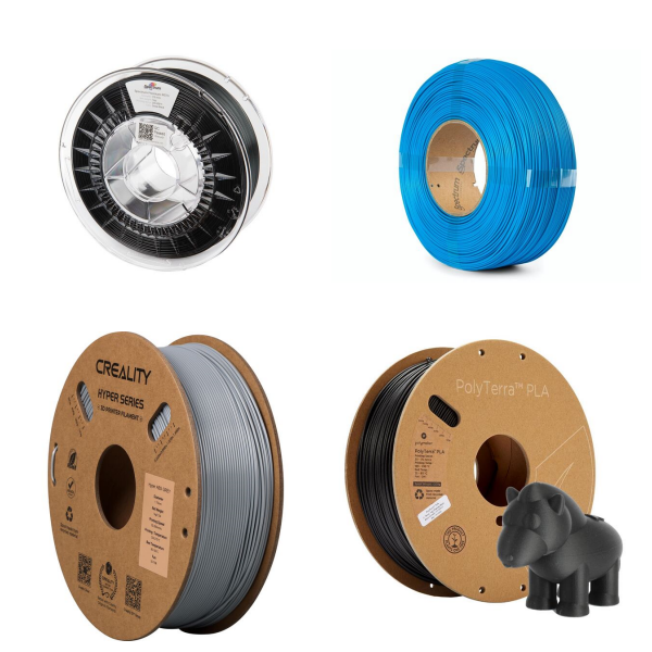
<h1> 3D Printing Materials </h1> <p> 3D printing filaments are solid strand thermoplastic feedstock for use in fused deposition construction of three-dimensional models using 3D printers. Filaments are differentiated by diameter, weight, tensile strength, flex strength, and density with common plastic formulations including ABS, PLA, PET, PA, PC, PS, PVA and TPU. Popular diameters are 1.75 mm, 2.85 mm, and 3.00 mm and are available in a wide range of solid and translucent colors. </p>
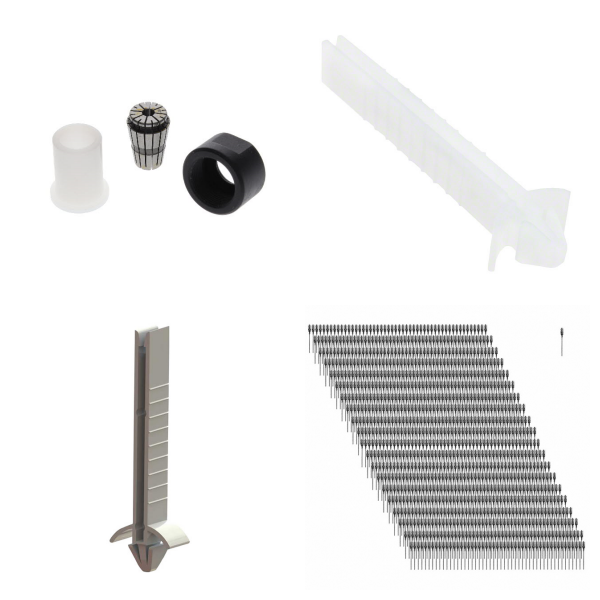
<h1> Accessories </h1> <p> Prototyping and fabrication accessories are designed to be used with related prototyping products such as circuit board guides, engraving machines, milling machines and more. Products in this category include items such as header pins, terminals, mounting kits and strips, polishing pads and tools. </p>
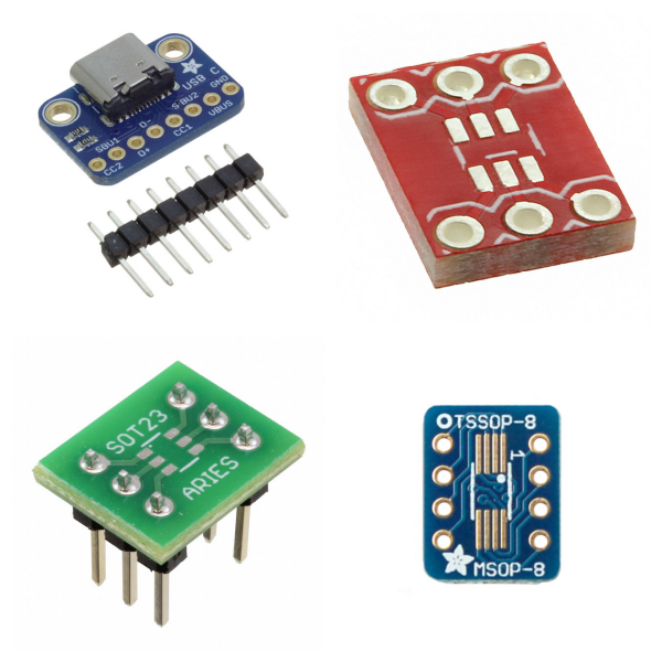
<h1> Adapter, Breakout Boards </h1> <p> Products in this family provide increased convenience of access to the electrical contacts of a connector, integrated circuit, or similar device by providing interconnection between a component placement area (typically for a fine-pitch, surface mounted integrated circuit) and an interconnect area typically having a much larger distance between pin centers. A common application is accommodating the use of solderless breadboards as a prototyping method for components that are not available in breadboard-compatible packaging. </p>
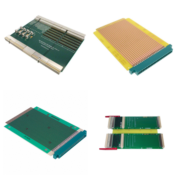
<h1> Card Extenders </h1> <p> Card Extenders are boards that have a card edge connector or contact pads on one or both sides of the card. These boards can then be populated with components and connectors for design and test purposes. </p>

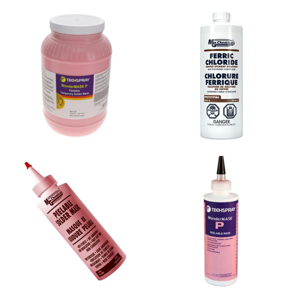
<h1> Coating, Grease, Repair </h1> <h2> 1. Coating </h2> <h3> 1) Technical Features: </h3> <p> Utilizing nano-scale composite coating materials, it offers high-temperature resistance (-40°C to 260°C), corrosion resistance (salt spray test ≥ 500h), and insulation resistance > 1012Ω. </p> <p> </p> <p> Products include conformal coatings (acrylic/polyurethane/silicone), conductive silver pastes, and optical coatings. </p> <p> </p> <h3> 2) Typical Applications: </h3> <p> ▶ PCB moisture-proofing (IPC-CC-830B compliant) </p> <p> ▶ Automotive electronics salt spray coating (AEC-Q100 certified) </p> <p> ▶ Radiation-resistant coatings for aerospace components (meets MIL-I-46058C requirements) </p> <p> </p> <h2> 2. Grease </h2> <h3> 1) Technology Matrix: </h3> <table> <tbody> <tr class="firstRow"> <td width="94" valign="top" style="padding: 0px 7px; border-width: 1px; border-color: windowtext; background: rgb(190, 190, 190);"> <p> Type </p> </td> <td width="139" valign="top" style="padding: 0px 7px; border-width: 1px; border-color: windowtext; background: rgb(190, 190, 190);"> <p> Operating Temperature Range </p> </td> <td width="162" valign="top" style="padding: 0px 7px; border-width: 1px; border-color: windowtext; background: rgb(190, 190, 190);"> <p> Base Oil Composition </p> </td> <td width="172" valign="top" style="padding: 0px 7px; border-width: 1px; border-color: windowtext; background: rgb(190, 190, 190);"> <p> Applications </p> </td> </tr> <tr style="height:58px"> <td width="94" valign="top" style="padding: 0px 7px; border-left-width: 1px; border-left-color: windowtext; border-right-width: 1px; border-right-color: windowtext; border-top: none; border-bottom-width: 1px; border-bottom-color: windowtext;"> <p> Silicone Grease </p> </td> <td width="139" valign="top" style="padding: 0px 7px; border-left-width: 1px; border-left-color: windowtext; border-right-width: 1px; border-right-color: windowtext; border-top: none; border-bottom-width: 1px; border-bottom-color: windowtext;"> <p> -50~200℃ </p> </td> <td width="162" valign="top" style="padding: 0px 7px; border-left-width: 1px; border-left-color: windowtext; border-right-width: 1px; border-right-color: windowtext; border-top: none; border-bottom-width: 1px; border-bottom-color: windowtext;"> <p> Dimethyl Silicone Oil </p> </td> <td width="172" valign="top" style="padding: 0px 7px; border-left-width: 1px; border-left-color: windowtext; border-right-width: 1px; border-right-color: windowtext; border-top: none; border-bottom-width: 1px; border-bottom-color: windowtext;"> <p> Precision Gears/Optical Instruments </p> </td> </tr> <tr style="height:69px"> <td width="94" valign="top" style="padding: 0px 7px; border-left-width: 1px; border-left-color: windowtext; border-right-width: 1px; border-right-color: windowtext; border-top: none; border-bottom-width: 1px; border-bottom-color: windowtext;"> <p> Fluoro Grease </p> </td> <td width="139" valign="top" style="padding: 0px 7px; border-left-width: 1px; border-left-color: windowtext; border-right-width: 1px; border-right-color: windowtext; border-top: none; border-bottom-width: 1px; border-bottom-color: windowtext;"> <p> -30~260℃ </p> <p> </p> </td> <td width="162" valign="top" style="padding: 0px 7px; border-left-width: 1px; border-left-color: windowtext; border-right-width: 1px; border-right-color: windowtext; border-top: none; border-bottom-width: 1px; border-bottom-color: windowtext;"> <p> Perfluoropolyether </p> </td> <td width="172" valign="top" style="padding: 0px 7px; border-left-width: 1px; border-left-color: windowtext; border-right-width: 1px; border-right-color: windowtext; border-top: none; border-bottom-width: 1px; border-bottom-color: windowtext;"> <p> Semiconductor Equipment Vacuum Chambers </p> </td> </tr> <tr style="height:31px"> <td width="94" valign="top" style="padding: 0px 7px; border-left-width: 1px; border-left-color: windowtext; border-right-width: 1px; border-right-color: windowtext; border-top: none; border-bottom-width: 1px; border-bottom-color: windowtext;"> <p> Conductive Grease </p> </td> <td width="139" valign="top" style="padding: 0px 7px; border-left-width: 1px; border-left-color: windowtext; border-right-width: 1px; border-right-color: windowtext; border-top: none; border-bottom-width: 1px; border-bottom-color: windowtext;"> <p> -40~150℃ </p> </td> <td width="162" valign="top" style="padding: 0px 7px; border-left-width: 1px; border-left-color: windowtext; border-right-width: 1px; border-right-color: windowtext; border-top: none; border-bottom-width: 1px; border-bottom-color: windowtext;"> <p> Synthetic Hydrocarbon + Silver Powder </p> </td> <td width="172" valign="top" style="padding: 0px 7px; border-left-width: 1px; border-left-color: windowtext; border-right-width: 1px; border-right-color: windowtext; border-top: none; border-bottom-width: 1px; border-bottom-color: windowtext;"> <p> Anti-oxidation for Electronic Contacts </p> </td> </tr> </tbody> </table> <p> </p> <h3> 2) Innovations: </h3> <p> • PTFE-containing food-grade grease (NSF H1 certified) </p> <p> • Graphene-enhanced thermal grease (thermal conductivity > 8W/m·K) </p> <p> </p> <h2> 3. Repair </h2> <h3> 1) Technical Solution: </h3> <p> Conductive Repair: Nanosilver Conductive Adhesive (Volume Resistivity < 5×10⁻⁴Ω·cm) </p> <p> Structural Repair: UV-curable Composite Material (Tensile Strength > 50MPa) </p> <p> Functional Repair: Self-healing Polymer Material (Self-healing Rate > 90% within 24 hours after damage) </p> <p> </p> <h3> 2) Industry Case Studies: </h3> <p> ✓ Drone PCB Wire Repair (Impedance Change < 3% After Repair) </p> <p> ✓ Industrial Robot Joint Regeneration (Extending Service Life by 2-3 Times) </p> <p> ✓ Photovoltaic Module Microcrack Repair (Restoring Power Generation Efficiency to 95%+) </p>
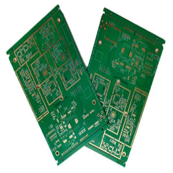
<h1> Custom Configurable PCB's </h1> <p> Custom Configurable Printed Circuit Boards (PCBs) are a core component of modern electronic design, designed to meet specific application requirements. Based on standard PCB (Printed Circuit Board) technology, they offer users tailored solutions by enabling highly flexible layout and component integration on the printed circuit board. This type of PCB allows designers to adjust the circuit structure, number of layers, and materials based on the device's size, function, or environmental requirements, enabling efficient system integration and shortening development cycles. </p> <p> </p> <p> <strong>Key Features</strong>: </p> <p> <strong>High Customizability</strong>: Users can customize circuit patterns, component layouts, and interconnections to suit diverse application scenarios, such as consumer electronics, industrial equipment, or medical devices. </p> <p> <strong>Systematic and Integrated Design</strong>: Electronic components are tightly integrated onto a single PCB, improving overall reliability and stability while reducing production costs and design complexity. </p> <p> <strong>Environmentally Friendly and Reliable</strong>: They are manufactured using environmentally friendly materials such as lead-free solder and undergo rigorous quality verification to ensure stable operation in high-voltage and high-frequency environments. </p> <p> </p> <p> In terms of application, this type of PCB is often used in scenarios requiring specific functions, such as low-frequency, high-voltage drive systems or wearable devices. By optimizing layout and material selection (such as metal substrates or multilayer designs), they meet the requirements of miniaturization and high density. </p> <p> </p> <p> Furthermore, its ease of repair and upgrade facilitates product lifecycle management, further enhancing market adaptability. For designers, mastering electromagnetic compatibility (EMC) analysis and thermal management techniques is key to ensuring performance, helping to address interference and heat dissipation challenges in complex environments. </p>
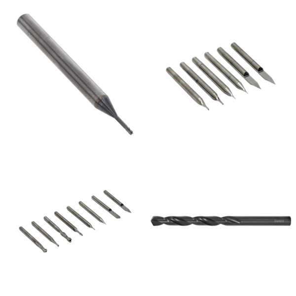
<h1> Drill Bits, End Mills </h1> <p> The cutting tool products within this family are primarily intended for the production of printed circuit boards by means of a mechanical milling process, though those tools adapted for drilling holes do so equally well on boards that have been chemically etched. Characteristic of this application is a relatively small tool size in comparison to those commonly found in household or industrial use. </p>
<h1> Etching and Fabrication Equipment </h1> <p> Etching and fabrication equipment is a core component of electronic component manufacturing, specializing in forming precise structures by removing material layers. It is widely used in fields such as semiconductors, optoelectronics, and integrated circuits. These devices ensure high precision, high integration, and reliable performance. </p> <p> </p> <h2> 1. Key Equipment and Technology Types </h2> <p> Etching and fabrication equipment encompasses a variety of advanced technologies, primarily including: </p> <p> </p> <p> <strong>Plasma Etching Equipment</strong>: Utilizes inductively coupled plasma (ICP) to achieve nanometer-level etching precision, suitable for semiconductor wafer processing. Key components, such as the focusing ring, use voltage to control plasma uniformity, improving chip yield. </p> <p> </p> <p> <strong>Photochemical Etching Equipment</strong>: Used for precision metal processing (such as titanium plates or circuit boards), it uses chemical solutions and photolithography to achieve micron-level etching, supporting customized production. </p> <p> </p> <p> <strong>Wet Etching Equipment</strong>: Involves the application of etchants in microfluidic systems, combined with photolithography to form channel networks, and is suitable for non-silicon-based materials. </p> <p> </p> <h2> 2. Core Functions and Application Scenarios </h2> <p> <strong>Etching equipment plays a key role in electronics manufacturing</strong>: </p> <p> </p> <p> <strong>Optoelectronic Device Fabrication</strong>: This encompasses photolithography, thin film deposition, and etching processes, supporting the development of devices such as lasers and detectors. Materials include non-silicon substrates such as gallium arsenide and gallium nitride. </p> <p> <strong> </strong> </p> <p> <strong>Semiconductor Manufacturing</strong>: Highly corrosion-resistant materials (such as silicon carbide) for components like focus rings extend equipment life and meet the demands of integrated circuit miniaturization. </p> <p> </p> <p> <strong>Resource Recycling and Environmental Protection</strong>: Developing recycling technologies for waste etching solutions (such as printed circuit board microetching solutions) enables efficient copper resource utilization and pollution control. </p> <p> </p> <h2> 3. Technological Advances and Future Directions </h2> <p> Global innovations in electronic materials are driving etching technology towards greener and more intelligent processes. For example, new focus ring materials such as boron carbide are pushing performance limits to meet the demands of high-power etching. </p>
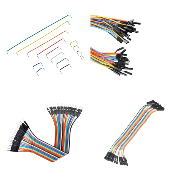
<h1> Jumper Wire </h1> <p> Products in the jumper wire family are primarily used in hobby or development contexts involving the use of solderless breadboards and/or interconnect systems based on common 0.1" (2.54 mm) pitch, square contact rectangular connectors. Available products include multi-conductor cables terminated with single- or multi-position connectors, insulated wires with ends pre-stripped and bent for breadboarding use, and assortments of the same in varying lengths and/or colors. </p>
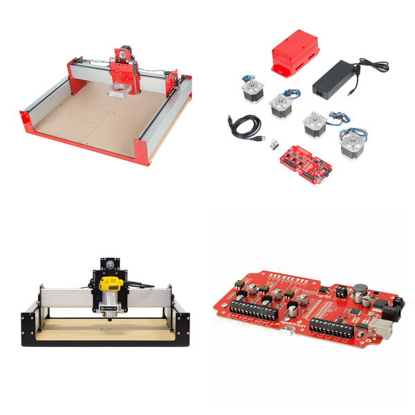
<h1> PCB Routers, Milling Machines </h1> <h2> 1. What are PCB Routers, Milling Machines? </h2> <p> PCB routers and milling machines are precision processing equipment used in the electronics manufacturing industry. They are primarily used for: </p> <p> High-precision PCB prototyping </p> <p> Rapid production of small batches of PCBs </p> <p> Processing of complex multilayer boards </p> <p> Contour cutting of special-shaped components </p> <p> </p> <h2> 2. Technical Parameters and Performance Indicators </h2> <table> <tbody> <tr style="height:31px" class="firstRow"> <td width="162" valign="top" style="padding: 0px 7px; border-width: 1px; border-color: windowtext; background: rgb(190, 190, 190);"> <p> Key Parameters </p> </td> <td width="195" valign="top" style="padding: 0px 7px; border-width: 1px; border-color: windowtext; background: rgb(190, 190, 190);"> <p> Industry Standard Range </p> </td> <td width="210" valign="top" style="padding: 0px 7px; border-width: 1px; border-color: windowtext; background: rgb(190, 190, 190);"> <p> Technology Evolution Trend </p> </td> </tr> <tr style="height:32px"> <td width="162" valign="top" style="padding: 0px 7px; border-left-width: 1px; border-left-color: windowtext; border-right-width: 1px; border-right-color: windowtext; border-top: none; border-bottom-width: 1px; border-bottom-color: windowtext;"> <p> Positioning Accuracy </p> </td> <td width="195" valign="top" style="padding: 0px 7px; border-left-width: 1px; border-left-color: windowtext; border-right-width: 1px; border-right-color: windowtext; border-top: none; border-bottom-width: 1px; border-bottom-color: windowtext;"> <p> ±0.01-0.025mm </p> </td> <td width="210" valign="top" style="padding: 0px 7px; border-left-width: 1px; border-left-color: windowtext; border-right-width: 1px; border-right-color: windowtext; border-top: none; border-bottom-width: 1px; border-bottom-color: windowtext;"> <p> Submicron Control System </p> </td> </tr> <tr style="height:15px"> <td width="162" valign="top" style="padding: 0px 7px; border-left-width: 1px; border-left-color: windowtext; border-right-width: 1px; border-right-color: windowtext; border-top: none; border-bottom-width: 1px; border-bottom-color: windowtext;"> <p> Spindle Speed </p> </td> <td width="195" valign="top" style="padding: 0px 7px; border-left-width: 1px; border-left-color: windowtext; border-right-width: 1px; border-right-color: windowtext; border-top: none; border-bottom-width: 1px; border-bottom-color: windowtext;"> <p> 30,000-100,000rpm </p> </td> <td width="210" valign="top" style="padding: 0px 7px; border-left-width: 1px; border-left-color: windowtext; border-right-width: 1px; border-right-color: windowtext; border-top: none; border-bottom-width: 1px; border-bottom-color: windowtext;"> <p> Air Bearing Spindle Popularization </p> </td> </tr> <tr style="height:32px"> <td width="162" valign="top" style="padding: 0px 7px; border-left-width: 1px; border-left-color: windowtext; border-right-width: 1px; border-right-color: windowtext; border-top: none; border-bottom-width: 1px; border-bottom-color: windowtext;"> <p> Processing Thickness </p> </td> <td width="195" valign="top" style="padding: 0px 7px; border-left-width: 1px; border-left-color: windowtext; border-right-width: 1px; border-right-color: windowtext; border-top: none; border-bottom-width: 1px; border-bottom-color: windowtext;"> <p> 0.1-10mm </p> </td> <td width="210" valign="top" style="padding: 0px 7px; border-left-width: 1px; border-left-color: windowtext; border-right-width: 1px; border-right-color: windowtext; border-top: none; border-bottom-width: 1px; border-bottom-color: windowtext;"> <p> Ultra-thin Sheet Compatibility </p> </td> </tr> <tr> <td width="162" valign="top" style="padding: 0px 7px; border-left-width: 1px; border-left-color: windowtext; border-right-width: 1px; border-right-color: windowtext; border-top: none; border-bottom-width: 1px; border-bottom-color: windowtext;"> <p> Minimum Line Width </p> </td> <td width="195" valign="top" style="padding: 0px 7px; border-left-width: 1px; border-left-color: windowtext; border-right-width: 1px; border-right-color: windowtext; border-top: none; border-bottom-width: 1px; border-bottom-color: windowtext;"> <p> 0.1-0.3mm </p> </td> <td width="210" valign="top" style="padding: 0px 7px; border-left-width: 1px; border-left-color: windowtext; border-right-width: 1px; border-right-color: windowtext; border-top: none; border-bottom-width: 1px; border-bottom-color: windowtext;"> <p> Laser Hybrid Processing Technology </p> </td> </tr> </tbody> </table> <p> </p> <h2> 3. What are the Typical Application Scenarios of PCB Routers, Milling Machines? </h2> <p> R&D and Verification Phase </p> <p> Design verification completed within 24 hours </p> <p> Supports processing of special materials such as FR4 and aluminum substrates </p> <p> </p> <p> Education and Research </p> <p> Electronic Engineering Teaching Experimental Equipment </p> <p> Tools for rapid iteration of scientific research projects </p> <p> </p> <p> Military and Aerospace Applications </p> <p> Meets IPC-6012 Class 3 standards </p> <p> Specialty material processing capabilities </p> <p> </p> <h2> 4. Key Points for Purchasing PCB Routers, Milling Machines </h2> <p> <strong>Users are advised to focus on</strong>: </p> <p> Dynamic machining accuracy and stability </p> <p> Automatic tool changing system </p> <p> Dust collection efficiency </p> <p> CAM software compatibility </p> <p> Equipment vibration suppression technology </p> <p> </p> <h2> 5. Industry Frontiers of PCB Routers, Milling Machines </h2> <p> <strong>Technical Breakthroughs in 2025</strong>: </p> <p> 5G millimeter wave PCB processing technology </p> <p> Embedded component cavity processing technology </p> <p> AI-driven adaptive milling algorithm </p>
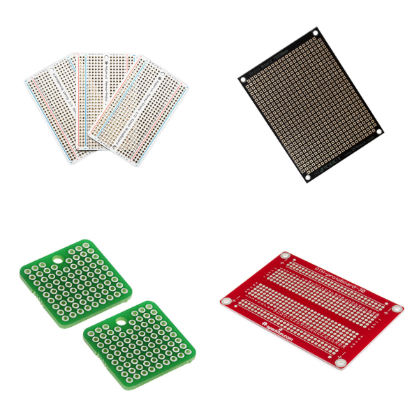
<h1> Prototype Boards Perforated </h1> <p> Perforated prototype boards are a common electronic prototyping tool, primarily used for the rapid construction and testing of circuit designs. They allow engineers and hobbyists to insert and solder electronic components directly onto the board, enabling preliminary circuit verification. </p> <p> </p> <h2> 1. What are the Features of Prototype Boards Perforated? </h2> <p> These boards feature evenly distributed small holes (perforations) across their surface, which are used to secure components and connect circuits. They eliminate the need for pre-designed copper foil layers and are suitable for small-scale or experimental projects. Perforated prototype boards are typically made of insulating materials (such as epoxy or fiberglass) to provide mechanical support and electrical isolation, ensuring safe and stable circuit assembly. </p> <p> </p> <h2> 2. What are the Main Types of Prototype Boards Perforated? </h2> <p> <strong>Single-sided Boards</strong>: Suitable for simple circuit designs, they are low-cost and have perforations on only one side, making them easy for beginners to quickly get started. </p> <p> </p> <p> <strong>Double-sided Boards</strong>: Supporting more complex circuit layouts, they feature perforations on both sides, allowing for interlayer connections through plated holes and increased design flexibility. </p> <p> </p> <p> <strong>Donut-style Boards</strong>: Circular perforated holes facilitate symmetrical component placement and are often used for small devices or modular prototypes, simplifying component alignment. </p> <p> </p> <p> The choice of these boards should be optimized based on project complexity, cost budget, and space requirements. </p> <p> </p> <h2> 3. What are the Applications of Prototype Boards Perforated? </h2> <p> In practice, the core purpose of perforated prototyping boards is to accelerate circuit prototyping development: </p> <p> </p> <p> They enable rapid design iterations, allowing engineers to test circuit functionality directly on the board, avoiding the long lead times and high costs of PCB production. They are particularly suitable for educational, DIY projects, and pre-product development, allowing for hand soldering to establish electrical connections and verify design feasibility. </p> <p> </p> <h2> 4. What are the Usage Steps of Prototype Boards Perforated? </h2> <p> </p> <p> <strong>Circuit Design</strong>: Plan the layout on paper or in software to ensure optimal component placement and efficient wiring. </p> <p> </p> <p> <strong>Component Insertion</strong>: Gently insert the component leads into the perforations, ensuring a tight fit to prevent loose connections. </p> <p> </p> <p> <strong>Soldering</strong>: Heat the connection points with a soldering iron to melt the solder and form a secure joint. Carefully control the temperature and amount of solder to ensure reliability. </p> <p> </p> <p> <strong>Pin Trimming</strong>: Remove excess pins after soldering to maintain a neat assembly and reduce the risk of short circuits. </p> <p> </p> <p> <strong>Circuit Testing</strong>: Thoroughly test functionality and performance after assembly to ensure it meets design requirements. </p> <p> </p> <p> The advantages of perforated prototyping boards include shortened development time, lower production costs (by reducing the number of PCB prototype iterations), and early detection of design flaws. Despite the widespread use of modern PCB technologies (such as flex and rigid-flex), perforated prototyping boards remain important for electronics entry and rapid verification due to their convenience and low cost. </p>
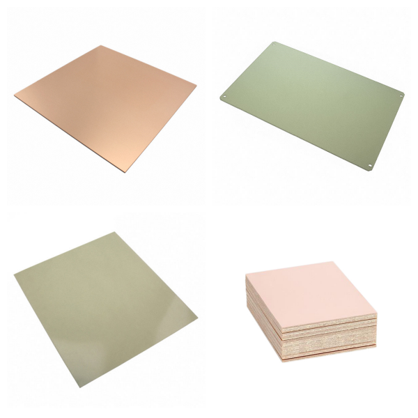
<h1> Prototype Boards Unperforated </h1> <h2> 1. What are Prototype Boards Unperforated? </h2> <p> A non-hole prototyping board refers to a circuit test substrate without standard through-holes or array-style sockets. Unlike breadboards with sockets, its core function is to provide electronics engineers with a customized circuit verification platform. Circuit traces must be formed through etching or printing processes. </p> <p> </p> <h2> 2. What are the Core Features of Prototype Boards Unperforated? </h2> <p> <strong>Structural Integrity</strong>: A fully copper-clad substrate with no pre-formed holes allows for precise circuit routing through photolithography or chemical etching, resulting in electrical characteristics that more closely resemble those of the final PCB. </p> <p> </p> <p> <strong>Professional Verification Scenarios</strong>: Suitable for complex verification tasks requiring simulation of real-world PCB environments, such as high-frequency circuits, high-current designs, and electromagnetic compatibility (EMC) testing. </p> <p> </p> <p> <strong>Manufacturing Process Relevance</strong>: Its design must adhere to PCB production process specifications (such as line width/spacing tolerances) to ensure that prototype test results can directly guide mass production. </p> <p> </p> <h2> 3. Comparison with Perforated Prototype Boards </h2> <table> <tbody> <tr class="firstRow"> <td width="114" valign="top" style="padding: 0px 7px; border-width: 1px; border-color: windowtext; background: rgb(190, 190, 190);"> <p> Features </p> </td> <td width="218" valign="top" style="padding: 0px 7px; border-width: 1px; border-color: windowtext; background: rgb(190, 190, 190);"> <p> Non-perforated Prototype Boards </p> </td> <td width="236" valign="top" style="padding: 0px 7px; border-width: 1px; border-color: windowtext; background: rgb(190, 190, 190);"> <p> Perforated Breadboards </p> </td> </tr> <tr style="height:49px"> <td width="114" valign="top" style="padding: 0px 7px; border-left-width: 1px; border-left-color: windowtext; border-right-width: 1px; border-right-color: windowtext; border-top: none; border-bottom-width: 1px; border-bottom-color: windowtext;"> <p> Connection Method </p> </td> <td width="218" valign="top" style="padding: 0px 7px; border-left-width: 1px; border-left-color: windowtext; border-right-width: 1px; border-right-color: windowtext; border-top: none; border-bottom-width: 1px; border-bottom-color: windowtext;"> <p> Etched copper traces </p> </td> <td width="236" valign="top" style="padding: 0px 7px; border-left-width: 1px; border-left-color: windowtext; border-right-width: 1px; border-right-color: windowtext; border-top: none; border-bottom-width: 1px; border-bottom-color: windowtext;"> <p> Jack-type physical contacts </p> </td> </tr> <tr style="height:54px"> <td width="114" valign="top" style="padding: 0px 7px; border-left-width: 1px; border-left-color: windowtext; border-right-width: 1px; border-right-color: windowtext; border-top: none; border-bottom-width: 1px; border-bottom-color: windowtext;"> <p> Reusability </p> </td> <td width="218" valign="top" style="padding: 0px 7px; border-left-width: 1px; border-left-color: windowtext; border-right-width: 1px; border-right-color: windowtext; border-top: none; border-bottom-width: 1px; border-bottom-color: windowtext;"> <p> Single-use (customization required) </p> </td> <td width="236" valign="top" style="padding: 0px 7px; border-left-width: 1px; border-left-color: windowtext; border-right-width: 1px; border-right-color: windowtext; border-top: none; border-bottom-width: 1px; border-bottom-color: windowtext;"> <p> Multiple plug-in/plug-out reuse </p> </td> </tr> <tr> <td width="114" valign="top" style="padding: 0px 7px; border-left-width: 1px; border-left-color: windowtext; border-right-width: 1px; border-right-color: windowtext; border-top: none; border-bottom-width: 1px; border-bottom-color: windowtext;"> <p> Signal Integrity </p> </td> <td width="218" valign="top" style="padding: 0px 7px; border-left-width: 1px; border-left-color: windowtext; border-right-width: 1px; border-right-color: windowtext; border-top: none; border-bottom-width: 1px; border-bottom-color: windowtext;"> <p> High (close to real PCB) </p> </td> <td width="236" valign="top" style="padding: 0px 7px; border-left-width: 1px; border-left-color: windowtext; border-right-width: 1px; border-right-color: windowtext; border-top: none; border-bottom-width: 1px; border-bottom-color: windowtext;"> <p> Suitable for low- to medium-frequency applications (contact impedance influences) </p> </td> </tr> <tr> <td width="114" valign="top" style="padding: 0px 7px; border-left-width: 1px; border-left-color: windowtext; border-right-width: 1px; border-right-color: windowtext; border-top: none; border-bottom-width: 1px; border-bottom-color: windowtext;"> <p> Applicable Scenarios </p> </td> <td width="218" valign="top" style="padding: 0px 7px; border-left-width: 1px; border-left-color: windowtext; border-right-width: 1px; border-right-color: windowtext; border-top: none; border-bottom-width: 1px; border-bottom-color: windowtext;"> <p> Pre-production functional/reliability verification </p> </td> <td width="236" valign="top" style="padding: 0px 7px; border-left-width: 1px; border-left-color: windowtext; border-right-width: 1px; border-right-color: windowtext; border-top: none; border-bottom-width: 1px; border-bottom-color: windowtext;"> <p> Quickly build basic circuits </p> <p> </p> </td> </tr> </tbody> </table> <p> </p> <h2> 4. Application Value of Perforated Prototype Boards </h2> <p> Non-perforated prototyping boards can expose design flaws (such as insufficient heat dissipation and signal interference) early on, reducing the risk of production failure by over 60% and shortening product time-to-market. For example, in the development of automotive electronic controllers, high-temperature vibration testing using these prototyping boards is essential to ensure component stability in extreme environments. </p> <p> </p>
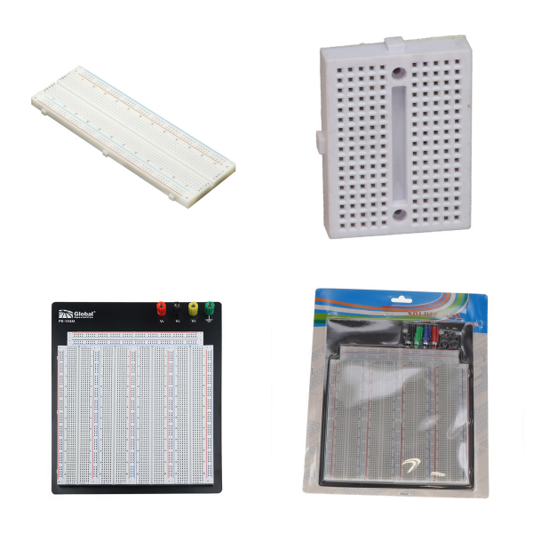
<h1> Solderless Breadboards </h1> <p> Solderless breadboard products provide a convenient means of interconnecting electronic components in hobby, educational, or development contexts, without the need for soldering or similar fixation processes. Composed of U-shaped metallic contacts positioned beneath a grid of holes in an electrically insulating housing, component leads, and wire segments inserted through the holes in the insulator are electrically connected and retained under spring tension by the contacts beneath. Though easily reconfigurable and thus ideal for experimentation, they do not provide mechanically robust interconnections, and introduce significant parasitic circuit elements which make them ill-suited for high-speed circuits. </p>
Prototyping, Fabrication Products
Prototyping and manufacturing products include materials and tools used to assemble small quantities of electronic circuits for development, research, repair, or similar purposes. Examples include solderless breadboards and adapters (for use with surface mount integrated circuits), perforated and non-perforated circuit board materials, and tools for producing printed circuit boards using chemical or mechanical processing techniques.