PCB Design Checklist: 15 Rules for Perfect Layouts
Printed Circuit Board (PCB) layout is arguably one of the most critical phases in electronic product development.
It’s where abstract schematic diagrams transform into a tangible foundation for your electronic circuit.
A meticulously designed PCB ensures optimal performance, minimizes electromagnetic interference (EMI), reduces manufacturing costs, and significantly enhances overall system reliability.
Conversely, a single oversight can lead to costly respins, signal integrity issues, and product failures, costing thousands of dollars and weeks of development time.
Whether you’re crafting a simple embedded system or a complex multi-layer board handling high-speed signals, a comprehensive PCB design checklist is not just helpful—it’s essential.
This guide provides an ultimate PCB design checklist, detailing 15 essential rules every engineer must know to achieve flawless layouts.
Following these rules will help you:
- Streamline your design process
- Improve manufacturer collaboration
- Optimize functionality and manufacturability from day one
1. The Foundation: Why a Checklist Matters
In the fast-paced world of electronics, even seasoned engineers can overlook crucial details. This is precisely why a PCB design checklist is indispensable.
It serves as a systematic verification framework, helping engineering teams catch potential design issues before fabrication.
Imagine spending weeks on a design, only to discover during assembly that critical components don’t fit, power traces are undersized, or EMC requirements were missed. Such scenarios highlight the immense value of a structured review process.
An effective PCB design checklist aids in:
- Averting design gaps and conflicts with PCB assembly services.
- Optimizing the placement of electrical components for performance and thermal management.
- Enhancing reliability and ease of manufacturability, reducing manufacturing issues.
- Accelerating prototyping and mass production by minimizing respins.
- Ensuring adherence to electrical, mechanical, and manufacturing requirements on the first pass.
As boards become more complex and manufacturing costs rise, the stakes for getting it right the first time have never been higher. Let’s dive into the essential rules that form the backbone of a perfect PCB layout.
2. The Ultimate PCB Design Checklist: 15 Essential Rules
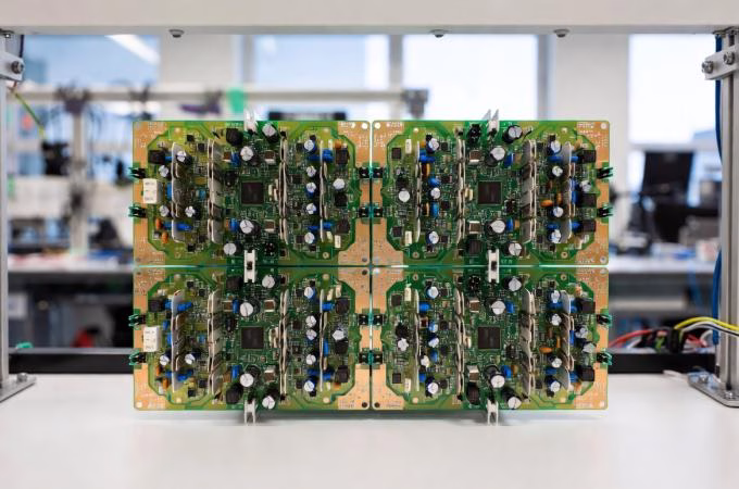
Rule 1: Strategic Component Placement
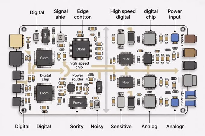
The foundation of any successful PCB layout begins with intelligent component placement. Group related components together, keep high-speed components close to their connectors, and minimize trace lengths for critical signals. Consider the signal flow, thermal dissipation, and mechanical constraints. Components requiring high current should be placed near the power source. Avoid placing noisy components near sensitive analog circuitry.
Rule 2: Define Layer Stackup and Materials
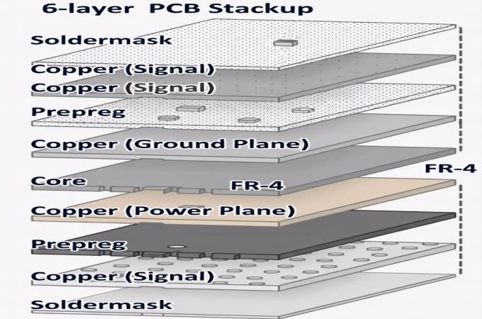
Before routing, carefully plan your PCB layer stackup. A well-designed stackup provides dedicated ground and power planes, controlled impedance for high-speed signals, and effective EMI shielding. Consider the number of layers (e.g., 4-layer for mixed signals, 6+ for high-speed/density) and materials (FR-4 is standard, but Rogers or PTFE might be needed for RF/microwave applications due to their specific dielectric properties). Proper stackup is crucial for signal integrity.
Rule 3: Establish Clear Design Rules and Constraints
Set up your design rules in your EDA software early on. This includes trace width and spacing, clearances (trace-to-pad, trace-to-via, component-to-component), minimum annular ring, drill sizes, and solder mask expansion . These rules are vital for manufacturability and electrical performance. Adhering to these rules prevents manufacturing defects and ensures the board meets its operational specifications.
Rule 4: Manage Signal Traces for Integrity
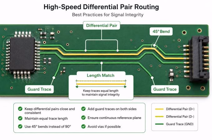
Keep all signal traces as short and direct as possible. Avoid sharp 90-degree bends, which can cause reflections and impedance discontinuities; use 45-degree bends or arcs instead. For high-speed signals, maintain controlled impedance and use differential pairs for signals like USB, Ethernet, or PCI Express, ensuring tight coupling and equal length matching to minimize common-mode noise.
Rule 5: Implement Solid Ground and Power Planes
Utilize solid ground planes to provide a low-impedance return path for signals and to reduce EMI. Similarly, solid power planes ensure stable voltage distribution. Avoid breaking ground planes unnecessarily, as this can force return currents to take longer, uncontrolled paths, leading to noise and cross-talk. Connect all ground pads directly to the ground plane with vias where necessary.
Rule 6: Decoupling and Bypass Capacitors
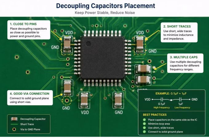
Place decoupling (or bypass) capacitors as close as possible to the power pins of integrated circuits (ICs), especially high-speed digital ICs and FPGAs. These capacitors provide localized reservoirs of charge, filtering noise and stabilizing power supply rails. Use appropriate capacitance values and minimize trace lengths to the IC pins for maximum effectiveness.
Rule 7: Address High-Speed Signal Requirements
For high-speed signals (above 50 MHz or with fast rise times), consider termination resistors, length matching, and careful routing to prevent reflections and timing issues. Implement guard traces for sensitive analog signals or high-frequency traces to provide isolation from noise sources. Understanding the critical length of your signals is key to determining if these measures are necessary.
Rule 8: Ensure Power Integrity (PI)
Power integrity goes hand-in-hand with signal integrity. Ensure power traces are wide enough to handle the maximum current draw without excessive voltage drop or overheating. Use power planes where possible for robust power delivery. Analyze current densities to identify potential bottlenecks and ensure sufficient copper for current flow.
| Issue | Impact on Performance | Mitigation Strategy |
| Voltage Drop | Reduced device performance, logic errors | Wider power traces/planes, multiple vias, sense lines |
| Ground Bounce | False switching, EMI generation | Solid ground planes, effective decoupling |
| IR Drop | Localized heating, power loss | Optimize trace widths based on current density |
Rule 9: Minimize EMI/EMC Issues
Electromagnetic compatibility (EMC) is crucial for product compliance and reliable operation. Beyond good grounding and stackup, use techniques like shielding sensitive traces, careful placement of filtering components, and ensuring proper chassis grounding. Minimize loop areas for all high-frequency current paths. Isolate analog and digital grounds where possible, connecting them at a single point.
Rule 10: Thermal Management
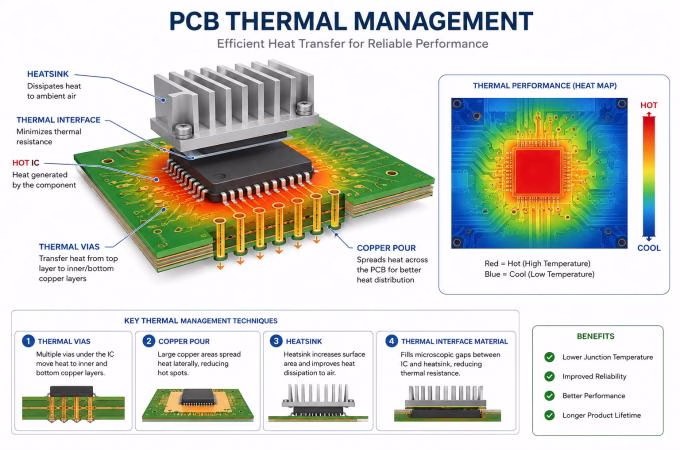
High-power components generate heat, which can degrade performance and reduce component lifespan. Incorporate thermal management strategies such as adequate spacing between heat-generating components, using thermal vias to dissipate heat to inner layers or heatsinks, and considering copper pours for heat spreading. Simulate thermal performance if needed for critical designs.
3. Mastering Manufacturability: DFM and DFA
Rule 11: Design for Manufacturability (DFM)
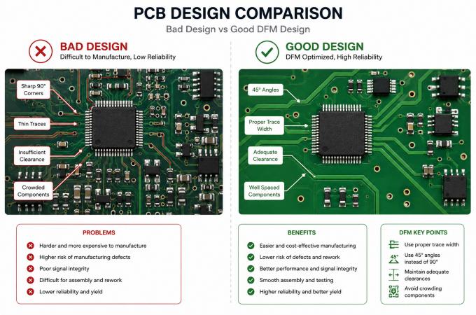
DFM focuses on making your PCB easy and cost-effective to fabricate. This includes adhering to minimum trace widths and spacing, ensuring adequate annular rings for vias and pads, correct pad-to-paste ratios, and proper solder mask clearances.Consult your manufacturer’s capabilities early in the design process. View our full PCB manufacturing capabilities and request a free DFM review to avoid costly issues.
Small deviations from DFM guidelines can significantly increase manufacturing costs or lead to failures. Request a free DFM review from our team before finalizing your design.
Rule 12: Design for Assembly (DFA)
DFA considers the ease of placing and soldering components during assembly. Ensure sufficient spacing between components for automated pick-and-place machines and for hand soldering if required. Clearly define silkscreen markings for component outlines, polarity indicators, and pin 1 locations. Proper component orientation can also reduce assembly time and errors.
Rule 13: Via Management
Vias are essential for connecting different layers, but their improper use can cause issues. Minimize the number of vias, especially on high-speed traces, as each via introduces an impedance discontinuity. Choose appropriate via types (through-hole, blind, buried) based on layer count and signal requirements. Ensure vias meet aspect ratio requirements from your manufacturer to prevent drilling problems.
4. Verification and Documentation: The Final Frontier
Rule 14: Perform Thorough Design Rule Checks (DRC)
Before sending your board for fabrication, run a comprehensive Design Rule Check (DRC) in your EDA software. This automated process verifies that your layout adheres to all specified electrical and manufacturing rules. Supplement automated checks with a manual visual inspection, focusing on critical areas like high-speed routing, power distribution, and component clearances. A pre-release review of placement, routing, stackup, SI/PI, EMC, and DFM/DFA can significantly reduce respins.
Rule 15: Document Everything
Good documentation is crucial for manufacturing, assembly, testing, and future revisions. Ensure your design files (Gerber files, drill files, BOM, assembly drawings, fabrication notes) are complete, accurate, and clearly labeled. Include any specific instructions for assembly or testing. This meticulous documentation accelerates prototyping and mass production, and helps avoid conflicts with PCB assembly services.
Ensure your design files (Gerber files, drill files, BOM, assembly drawings) are complete. Upload your files and get a quote today.
5. FAQ
- Question 1:What is the most common mistake beginners make in PCB design?
Answer: One of the most common mistakes is insufficient planning, especially regarding component placement and layer stackup. Rushing these initial steps often leads to signal integrity issues, poor thermal management, and difficulty in routing, requiring costly redesigns. - Question 2:How often should I refer to a PCB design checklist?
Answer: A checklist should be referenced at multiple stages: during initial planning, throughout the layout process, and critically, as a final review before releasing files for manufacturing. For complex designs, it’s beneficial to review sections iteratively. - Question 3:What’s the difference between DFM and DFA?
Answer: DFM (Design for Manufacturability) focuses on optimizing the design for the fabrication process (e.g., trace widths, clearances, drill sizes). DFA (Design for Assembly) focuses on making the board easy to populate with components (e.g., component spacing, silkscreen clarity, pad sizes for soldering). Both are crucial for reducing costs and improving yield. - Question 4:Can I ignore some of these rules for simple boards?
Answer: While some rules (e.g., high-speed signal specificities) might be less critical for very simple, low-frequency boards, core principles like good component placement, solid grounding, and DFM/DFA remain essential for reliability and manufacturability regardless of complexity. It’s best practice to always consider all rules.
6. Summary
A flawless PCB layout is the cornerstone of a reliable and high-performing electronic product. By diligently following these 15 essential PCB design rules, engineers can significantly improve their design quality, minimize manufacturing errors, and enhance overall product reliability.
From strategic component placement and meticulous stackup definition to rigorous DFM/DFA considerations and comprehensive final verification, each step in this checklist plays a vital role.
Embracing a structured approach to PCB design ensures that your circuit board meets all electrical, mechanical, and manufacturing requirements on the first pass, saving time and resources in the long run.
7. Key Takeaways
- Plan Early:Component placement and layer stackup are foundational; get them right from the start to avoid costly downstream issues.
- Prioritize Integrity:Solid ground planes, proper decoupling, and careful high-speed routing are paramount for signal and power integrity.
- Design for Production:Always consider Design for Manufacturability (DFM) and Design for Assembly (DFA) to ensure cost-effective and reliable fabrication and assembly.
- Verify Thoroughly:Utilize automated DRCs and conduct manual visual inspections as a final crucial step before manufacturing release.
- Document Everything:Comprehensive documentation is key for manufacturing success, future revisions, and troubleshooting.
As part of the same trusted team,we are excited to introduce our brand:OrinewPCB for faster,high-quality One-Stop PCB assembly services.


