PCB Soldering: How to Solder a PCB

1. Introduction to PCB Soldering
Welcome to the exciting world of electronics! Whether you’re a budding hobby ist, an engineering student, or a seasoned technician looking to refine your skills, understanding how to solder a PCB is a fundamental skill. PCB soldering is the process of attaching electronic components onto a printed circuit board (PCB) using a molten metal alloy called solder. This process creates a strong, permanent electrical and mechanical bond, transforming a bare PCB into a functional Printed Circuit Assembly (PCA).
Many beginners find soldering intimidating, filled with questions about tools, temperatures, and techniques. However, with the right guidance and practice, you can master this craft and create reliable, long-lasting electronic circuits. This comprehensive guide will walk you through the essential steps, from setting up your workspace to troubleshooting common issues, ensuring you can solder a PCB like a pro. We’ll cover everything you need to know to create reliable joints without damaging your board or components.
2. Essential Tools & Materials for Soldering
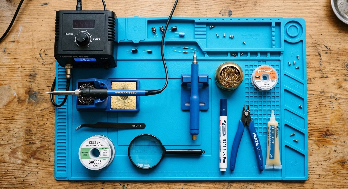
Before you even plug in your soldering iron, gathering the correct tools and materials is crucial for a successful and enjoyable experience. Using the right equipment will not only make the process easier but also significantly improve the quality and reliability of your solder joints.
Core Soldering Equipment
- Soldering Iron:This is your primary tool. Look for a pencil-shaped handheld iron , preferably with temperature control. A temperature range of 325-375°C (617-707°F) is ideal for most applications, preventing circuit board damage from excessive heat. Interchangeable tips (ch isel, conical, bevel) offer versatility for different component sizes and tasks.
- Solder Wire:The molten metal alloy used to form the electrical connection. Lead-free solder is highly recommended for health reasons, though leaded solder (60/40 or 63/37 tin/lead) is still used by some due to its lower melting point and easier flow. Many solders come with a rosin core, acting as a built-in flux.
- Flux:A chemical agent that cleans and prepares surfaces by removing oxidation, allowing solder to flow smoothly and form a strong bond. While some solder wire contains flux, a separate flux pen or paste can be very helpful for tough joints or pre-tinning.
- Soldering Iron Stand:Essential for safety, holding the hot iron securely when not in use. Many stands include a sponge or brass wool for tip cleaning.
Supporting Tools & Materials
- Desoldering Tools:Mistakes happen! A desoldering pump (solder sucker) or desoldering braid (wick) is invaluable for removing excess solder or correcting errors like cold solder joints or solder bridges.
- Tweezers:Fine-tipped tweezers are excellent for positioning small components, especially surface mount devices (SMD).
- Wire Cutters/Flush Cutters:Used to trim component leads after soldering, ensuring a neat finish and preventing short circuits.
- Safety Glasses:Protect your eyes from stray solder splashes or flying component leads.
- Fume Extractor/Fan:Sold ering fumes can be hazardous. A small fan or fume extractor helps clear the air in your workspace.
- Magnifying Glass or Bench Magnifier:Aids in inspecting small components and solder joints for quality.
- Helping Hand Tool/PCB Holder:A clamp with adjustable arms to hold your PCB steady, freeing up both hands for soldering.
3. Setting Up Your Workspace & Safety Protocols
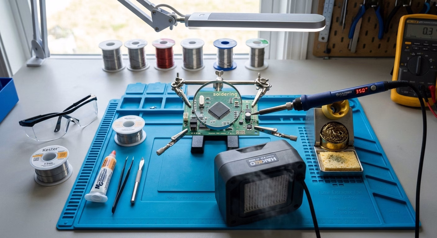
A well-prepared and safe workspace is paramount for efficient and effective soldering. It minimizes hazards and allows you to focus on the task at hand.
Workspace Setup
- Lighting:Ensure your workspace is brightly lit. Good visibility is crucial for seeing fine details on the PCB and identifying potential issues.
- Cleanliness:Keep your area clean and organized. Cluttered spaces can lead to accidents or lost components.
- Ventilation:This is critical. Soldering fumes contain harmful chemicals. Work in a well-ventilated area, preferably with a fume extractor or at least an open window and a fan to direct fumes away from your face.
- Surface Protection:Use a heat-resistant mat or surface protector to prevent damage to your workbench from accidental hot solder or iron contact.
- Static Protection:If working with sensitive electronic components, an anti-static mat and wrist strap can prevent damage from electrostatic discharge (ESD).
Safety Measures
- Eye Protection:Always wear safety glasses to protect against splashes of molten solder or flying clipped leads.
- Burn Prevention:The soldering iron tip can reach over 300°C. Always place it in its stand when not in use. Avoid touching the element or tip.
- Fire Safety :Keep flammable materials away from your soldering area. Have a small, accessible fire extinguisher (for electrical fires) or a cup of sand nearby, just in case.
- Lead Safety (if using leaded solder):If using leaded solder, avoid touching your face, eating, or drinking until you have thoroughly washed your hands. Ensure proper ventilation.
4. Pre-Soldering Preparation: Readying Your Components & Iron
Proper preparation significantly impacts the quality of your solder joints. Taking a few minutes to prepare your tools and materials can save you a lot of frustration later.
Circuit Board Surface Preparation
Ensure your PCB is clean and free of dirt, oil, or oxidation. You can use isopropyl alcohol and a lint-free cloth or a specialized PCB cleaner. Clean pads allow for better solder flow and stronger connections.
Soldering Iron Preparation (Tinning)
Tinning your soldering iron tip is a vital step. A clean, tinned tip ensures efficient heat transfer and prevents oxidation, which can hinder soldering.
- Heat the Iron:Turn on your soldering iron and let it reach its operating temperature (e.g., 350°C).
- Clean the Tip:Wipe the hot tip on a damp sponge (not soaking wet) or brass wool to remove any old solder or residue.
- Apply Fresh Solder:Immediately apply a small amount of fresh solder wire to the clean tip. The solder should melt and coat the tip evenly, giving it a shiny, silvery appearance. This protective layer prevents oxidation and improves heat transfer. If the tip doesn’t take solder or looks dull, repeat the cleaning and tinning process.
5. Step-by-Step PCB Soldering Process (Through-Hole)
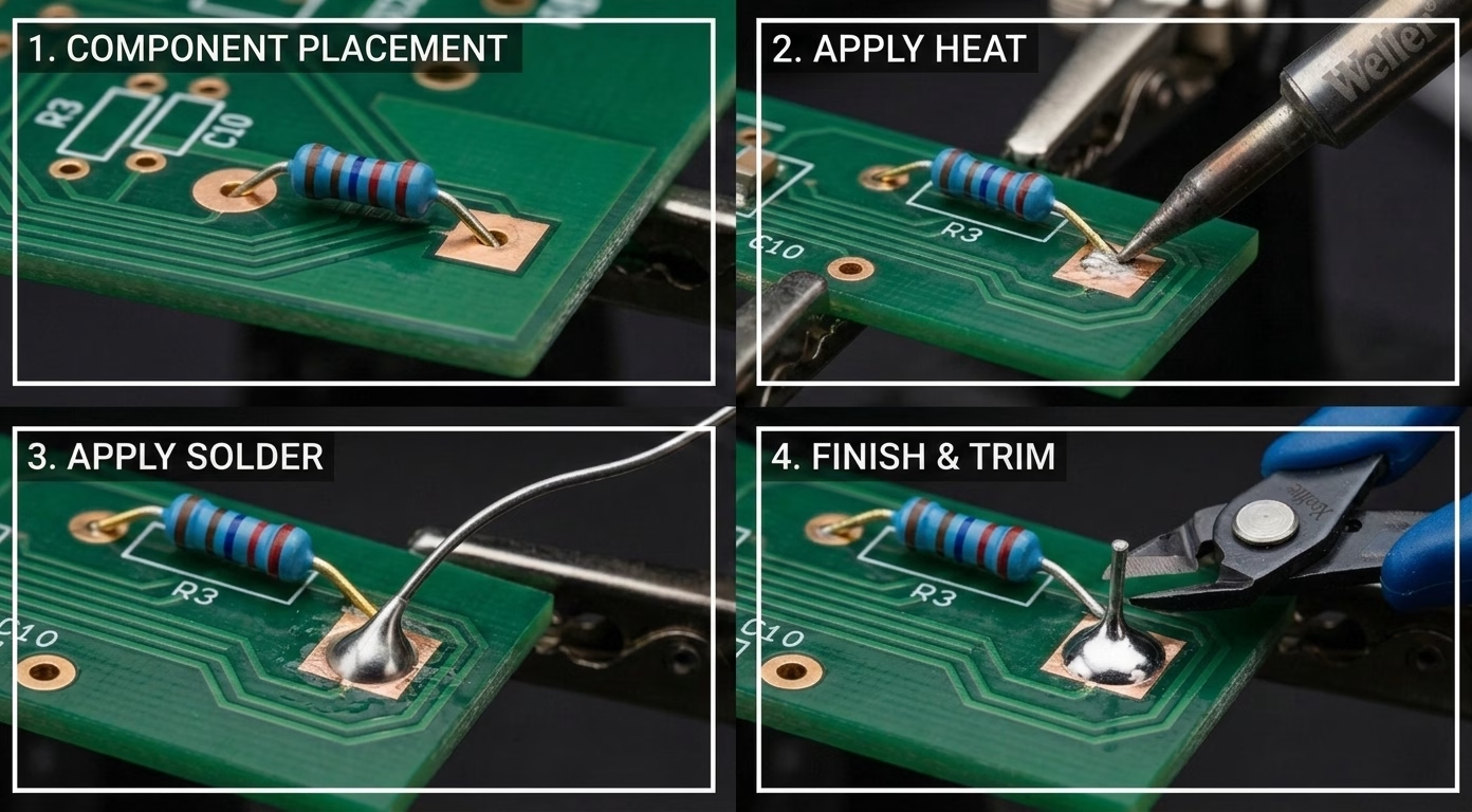
This guide focuses on through-hole components, which are generally easier for beginners. The technique is often described as a “three-second rule” or “heating, applying, removing.”
- Component Placement:
Insert your component into the correct holes on the PCB . Ensure it’s fully seated against the board. For stability during soldering, gently bend the component leads outwards at a slight angle (about 45 degrees) on the solder side of the board. This holds the component in place and prevents it from falling out. - Applying Heat:
Position the soldering iron tip so it simultaneously touches both the metal pad on the PCB and the component lead. This is crucial for even heat distribution . Hold the iron steadily for about 2-3 seconds, allowing both the pad and the lead to reach the solder’s melting temperature. You’ll often see the pad become slightly shiny as it heats up. - Applying Solder:
Once the pad and lead are heated, touch the end of your solder wire to the heated joint – specifically, where the iron tip, lead, and pad meet, but NOT directly to the iron tip itself. The heated components should melt the solder, causing it to flow smoothly around the lead and spread evenly over the pad, forming a conical or volcano shape. - Cooling & Removing:
As soon as enough solder has flowed to form a good joint (usually 1-2 seconds of solder application), first remove the solder wire, then remove the soldering iron. Allow the joint to cool naturally without disturbing the component. A good joint will solidify quickly and appear shiny and smooth. - Post-Soldering Inspection:
Carefully examine the solder joint. A good joint should be shiny, smooth, and concave (like a tiny volcano), covering both the component lead and the pad. There should be no gaps or holes. The component should be securely held in place. - Cleanup :
Once cooled, use your flush cutters to trim the excess component lead as close to the solder joint as possible, without cutting into the joint itself. Finally, if using rosin-core solder or flux, you may notice some sticky residue. This can be cleaned with isopropyl alcohol and a brush to ensure a professional finish and prevent future issues.
6. Troubleshooting Common Soldering Issues
Even experienced solderers encounter issues. Knowing how to identify and fix them is part of mastering the skill. Here are some common problems:
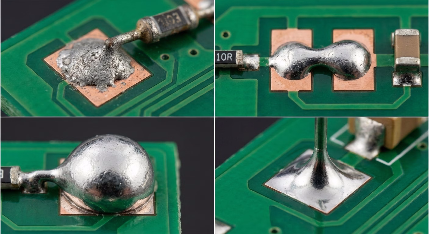
| Issue | Description & Cause | Solution |
| Cold Solder Joints | Dull, lumpy, grey, or rough appearance. Caused by insufficient heat or disturbance during cooling. Results in poor electrical connection. | Reheat the joint, apply a tiny amount of fresh solder (which contains flux), and allow it to flow smoothly before removing the iron and letting it cool undisturbed. |
| Solder Bridges | Solder accidentally connecting two or more adjacent pads or traces that should not be connected. Causes short circuits. | Use desoldering braid or a desoldering pump to remove the excess solder. Then, reheat the area, carefully dragging the iron across the bridge to clear it. |
| Pad Lifting | The copper pad detaches from the PCB substrate. Caused by excessive heat or prolonged heating. | This is difficult to repair. Avoid by using the correct temperature and limiting heat application time. If it happens, you might need to create a new connection point or run a jumper wire. |
| Poor Solder Flow | Solder balls up, doesn’t spread evenly, or adheres only to the lead or pad, but not both. Often due to insufficient heat, oxidized surfaces, or insufficient flux. | Ensure the iron tip is clean and tinned. Increase heat time slightly (but not excessively). Apply flux if necessary. Make sure both surfaces are clean. |
| Over-Soldering / “Blobbing” | Too much solder applied, forming a large, convex blob. Can hide poor connections or lead to bridges. | Use desoldering braid or a pump to remove the excess solder, then reflow the joint with a smaller amount of solder. |
7. Advanced Tips & Best Practices for Quality Joints
To move beyond basic soldering and ensure long-term reliability for your projects, consider these advanced tips:
- Practice Makes Perfect:Soldering is a skill that improves with experience. Don’t be afraid to practice on old circuit boards or beginner kits. The more you do it, the better your “feel” for the process will become.
- Heat Management:Always use the lowest effective temperature for your soldering iron. Excessive heat can damage components, lift pads, or char the PCB. The goal is to heat the joint quickly and efficiently.
- Tip Maintenance:Keep your iron tip clean and tinned at all times. A dirty or oxidized tip transfers heat poorly and leads to poor joints. Wipe it often on a damp sponge or brass wool and re-tin.
- Proper Solder Amount:Aim for just enough solder to form a smooth, concave fillet around the joint. Too little leads to weak connections; too much can hide problems or create bridges.
- Component Orientation:Pay close attention to the orientation of polarized components like diodes, LEDs, and electrolytic capacitors. Incorrect placement will prevent your circuit from working.
- Quality Control:Develop an eye for a good solder joint. Inspect every joint under magnification. A shiny, smooth, concave joint is your goal.
- Autom ated vs. Hand Soldering:While hand soldering is crucial for prototyping and repair, understand that mass production often utilizes automated processes like wave soldering or reflow ovens for consistency and speed.
8. Soldering Specific PCB Types (Briefly)
While the core principles remain, different PCB types and components might require slight variations in technique.
- Flexible PCBs (Flex Circuits):These require lower temperatures and quick soldering times due to their delicate polyimide substrate. Specialized low-temperature solders might be used.
- HDI PCBs (High-Density Interconnect):These boards feature tiny microvias and blind vias . Soldering on HDI PCBs often requires more precision and potentially finer tips or even hot air rework stations for very small components.
- Multilayer PCBs:These boards have internal layers, which means they can dissipate heat more quickly . You might need a slightly higher iron temperature or more dwell time to adequately heat the joint.
- Surface Mount Device (SMD) Soldering:This is a more advanced technique. Instead of through-hole leads , SMDs sit on top of the PCB pads.
- Manual SMD Soldering:You’ll typically use fine-tipped tweezers to position the SMD part. Apply a small amount of solder to one pad first ( tinning one pad). Hold the part with tweezers and reheat the tinned pad to attach one leg. Then, solder the remaining pads.
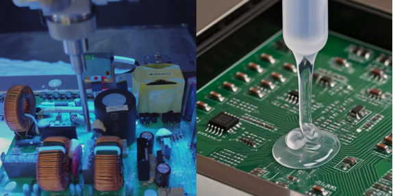
- Solder Paste & Hot Air:For multiple SMDs, solder paste can be applied to pads, components placed, and then heated with a hot air rework station or reflow oven.
9. PCB Soldering FAQ
(1) What’s the Difference Between PCB and PCA?
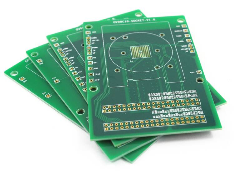
PCB (Printed Circuit Board) refers to the bare board with conductive paths, while PCA (Printed Circuit Assembly) is a PCB with soldered components. Soldering transforms a PCB into a functional PCA.
(2) How do I choose the right solder?
For beginners and general electronics, a rosin-core lead-free solder (e.g., Sn9 9.3/Cu0.7 or Sn96.5/Ag3.0/Cu0.5) is a good starting point due to health considerations. If you’re struggling with lead-free, 63 /37 tin/lead solder has a lower melting point and flows more easily, but requires proper ventilation and hand washing.
(3) My solder isn’t melting, or it’s not sticking. What’s wrong?
This is usually due to an unclean or improperly tinned soldering iron tip, insufficient heat, or oxidized surfaces on the component/PCB. Ensure your tip is shiny and tinned, that you’re heating both the pad and lead simultaneously, and that surfaces are clean (use flux if necessary).
10. Summary
Mastering PCB soldering is an achievable skill that opens up a world of electronic possibilities. From understanding your essential tools like the soldering iron to setting up a safe and efficient workspace, each step contributes to reliable results. The core process involves heating the joint (pad and component lead), applying solder, allowing it to flow, and then letting it cool undisturbed. By practicing, paying attention to heat management, and learning to troubleshoot common issues like cold solder joints or solder bridges, you’ll soon be confidently creating high-quality connections on any printed circuit board . Remember, “practice makes the master,” and every successful joint builds your expertise!
11. Key Takeaways
- Choose the right tools: A good temperature-controlled soldering iron , quality solder wire, and essential supporting tools are non-negotiable.
- Safety first: Always work in a well-ventilated area with eye protection, and ensure proper handling of hot equipment.
- Prepare properly : Clean your PCB and always keep your soldering iron tip clean and tinned for efficient heat transfer.
- Heat the joint, not the solder: Ensure both the component lead and the PCB pad are heated simultaneously before introducing solder.
- Aim for shiny, concave joints: A well-soldered joint should be smooth, shiny, and form a slight concave fillet.
- Learn from mistakes: Understand common issues like cold solder joints and solder bridges, and how to correct them using desoldering tools.
- Practice is key: Consistent practice will build your muscle memory and intuition, leading to improved quality control and speed.
