What is Wave Soldering? Your Guide to PCB Assembly

1. Introduction to Wave Soldering
In the vast and intricate world of electronics manufacturing, the assembly of Printed Circuit Boards (PCBs) is a foundational process. The reliability of electrical connections and the overall functional stability of electronic products hinge significantly on effective soldering. Among the various soldering technologies, wave soldering stands out as one of the earliest and most impactful methods for achieving large-scale automated production. Invented in the mid -1950s, this revolutionary technique was a catalyst for the electronics revolution, enabling the mass production of PCBs that transformed industries and daily life.
While the electronics industry has seen a significant shift towards Surface Mount Technology (SMT) in recent decades, wave soldering remains a critical, mature, and reliable soldering method. It continues to play an indispensable role, especially for components that lack SMT alternatives, require high mechanical strength, or are used in high-reliability fields such as industrial and automotive applications. This comprehensive guide will delve into the intricacies of wave soldering, exploring its mechanism, process, benefits, and continued relevance in modern electronics manufacturing.
2. What Exactly is Wave Soldering?
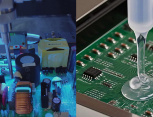
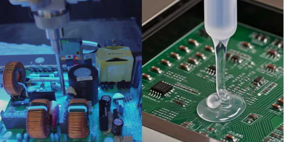
Wave soldering is an automated bulk soldering process predominantly used to solder through-hole components onto Printed Circuit Boards (PCBs). The fundamental principle involves passing a circuit board over a pan of molten solder, where a pump generates an “upwelling” or “standing wave” of solder. As the components’ leads on the underside of the PCB make contact with this molten wave, they are simultaneously soldered to the board, forming robust electrical and mechanical connections.
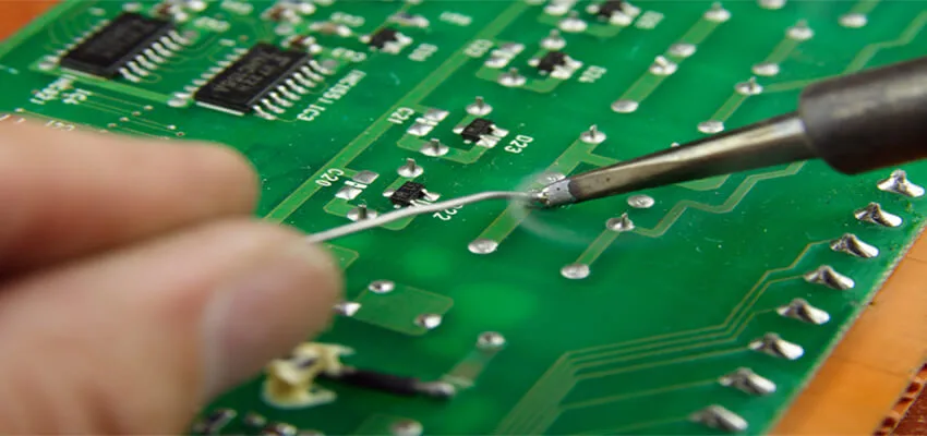
This method is characterized by its ability to solder hundreds of components onto a PCB in a matter of seconds, making it highly efficient for high-volume production. Even in assemblies that primarily utilize SMT components, wave soldering is often employed for attaching specific through-hole components like large capacitors, power devices, or high pin count connectors that are not suitable for reflow soldering. The process ensures both the electrical continuity and the mechanical strength required for the component attachments.
3. The Step-by-Step Wave Soldering Process
The wave soldering process is a highly automated sequence involving several crucial stages, each designed to prepare the PCB and components for a reliable solder joint. A conveyor system transports the PCB through these sequential zones:
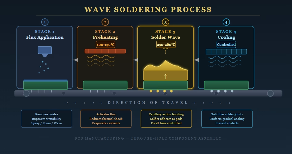
3.1. Flux Application
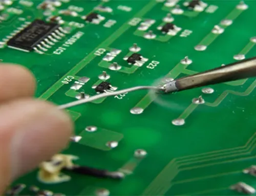
The initial stage involves applying a thin, uniform layer of flux to the bottom side of the PCB. Flux is a chemical cleaning agent essential for successful soldering. Its primary functions are to remove oxides from the metal surfaces of the PCB pads and component leads, prevent re-oxidation during preheating and soldering, and improve the wettability of the molten solder. This ensures a clean surface for the solder to adhere to, promoting strong, reliable joints. Flux can be applied via spraying, foaming, or wave application methods.
3.2. Preheating
After flux application, the PCB enters the preheating zone. The purpose of preheating is multifaceted:
- Activate the Flux:Elevated temperatures activate the flux , allowing it to effectively clean the metal surfaces.
- Reduce Thermal Shock:Gradually raising the PCB’s temperature minimizes the thermal shock that components would otherwise experience upon direct contact with the molten solder wave. This helps prevent damage to components and warpage of the PCB.
- Evaporate Solvents:It evaporates the volatile solvents in the flux, preventing solder ball formation and ensuring the flux’s non-volatile residues are left behind to protect the surface during soldering.
Preheating is typically achieved using radiant heaters, hot air, or a combination of both.
3.3. Soldering (Solder Wave)
This is the core stage where the actual soldering occurs. The preheated PCB passes over a pan of molten solder. A pump within the solder pot creates an upward-moving “wave” of solder. As the underside of the PCB, with its component leads protruding, comes into contact with this molten wave, the solder adheres to the exposed metal surfaces (pads and leads) due to capillary action and metallurgical bonding. The flux ensures excellent wettability, allowing the solder to flow and form strong, reliable joints. The interaction time, known as “dwell time,” is critical and carefully controlled.
3.4. Cooling
Immediately after passing through the solder wave, the PCB enters a cooling zone. Controlled cooling solidifies the solder joints, preventing movement of components while the solder is still molten and ensuring the formation of a strong, stable metallurgical bond. Rapid or uneven cooling can lead to defects, so this stage is often designed to cool the board uniformly and gradually.
4. Key Components of a Wave Soldering Machine
A typical wave soldering machine comprises several integrated sections working in harmony to facilitate the automated soldering process:
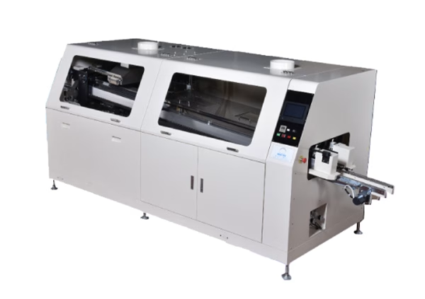
- Conveyor System:Transports the PCB uniformly through each stage of the machine at a controlled speed.
- Flux er:The section where flux is applied to the bottom of the PCB, typically using a spray, foam, or wave applicator.
- Preheater:Consists of heating elements (e.g., infrared heaters , hot air blowers) that raise the PCB’s temperature to activate the flux and reduce thermal shock.
- Solder Pot:A large reservoir containing molten solder, maintained at a precise temperature (typically between 25 0-265°C for lead-free solder).
- Solder Pump and Nozzle:A pump mechanism forces the molten solder upwards through a nozzle, creating the characteristic “wave” that the PCB passes over. Some machines feature dual waves (a turbulent wave and a laminar wave) for improved through-hole filling and defect reduction.
- Cooling Zone:Often equipped with fans or air jets to facilitate the controlled cooling and solidification of solder joints after the board exits the solder wave.
5. Advantages and Disadvantages of Wave Soldering
Despite the prevalence of newer technologies, wave soldering maintains a strong foothold due to its distinct advantages:
5.1. Advantages
- High Throughput:Ideal for mass production, capable of soldering hundreds of components quickly and efficiently.
- Strong Mechanical Joints:Excellent for through-hole components, creating robust mechanical and electrical connections, which is crucial for components requiring high reliability and structural integrity.
- Cost-Effective:For high-volume production of specific types of boards, it can be more economical than other methods.
- Suitable for Large Components:Effectively solders large, heavy, or irregularly shaped through-hole components that are challenging or impossible with SMT methods.
- Mature and Reliable Technology:Decades of refinement have made it a well-understood and highly dependable process.
5.2. Disadvantages
- Not Ideal for Fine-Pitch SMT:The turbulent nature of the solder wave can lead to bridging or short circuits on densely populated boards or fine-pitch surface mount devices.
- Higher Solder Usage:A large volume of molten solder is required, which can lead to higher material costs and dross formation.
- Potential for Defects:If not precisely controlled, defects such as solder bridges, icicling, voids, and insufficient hole fill can occur.
- Thermal Stress:Components are exposed to high temperatures, which can be a concern for temperature-sensitive parts.
- Environmental Impact:The use of flux and solder can generate fumes and dross that require proper ventilation and waste management.
6. Wave Soldering vs. Reflow Soldering
To understand wave soldering’s place in modern manufacturing, it’s helpful to compare it with its primary counterpart, reflow soldering. Reflow soldering is the dominant method for Surface Mount Technology (SMT) components, where solder paste is applied to pads, components are placed, and then the assembly is heated in an oven to melt and reflow the solder.
| Feature | Wave Soldering | Reflow Soldering |
| Component Type | Primarily Through-Hole (THT) | Primarily Surface Mount Technology (SMT) |
| Solder Application | Molten solder wave contacts PCB bottom | Solder paste applied to pads (before component placement) |
| Process | PCB passes over molten solder wave | PCB passes through heating zones in an oven to melt solder paste |
| Typical Applications | Large components, connectors, mixed-technology boards, high reliability | Dense SMT boards, fine-pitch components |
| Advantages | Strong mechanical joints, high throughput for THT | Fine-pitch capability, less thermal stress on components (often), precise control |
| Disadvantages | Less suitable for fine-pitch SMT, higher solder volume | Limited for large THT components, requires accurate solder paste printing |
While reflow soldering has largely supplanted wave soldering for pure SMT applications, wave soldering remains essential for boards with a mix of SMT and through-hole components, or those requiring the specific mechanical strength and reliability that THT soldering provides.
7. Common Applications of Wave Soldering
Despite the advancements in SMT, wave soldering continues to be a vital process in several key areas of electronics manufacturing:
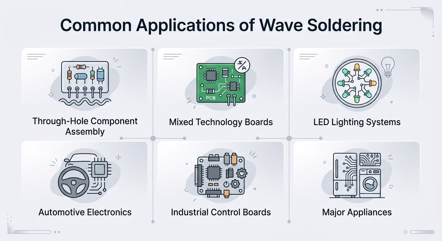
- Through-Hole Component Assembly:Its primary use, especially for components where mechanical robustness is paramount, such as large connectors, relays, switches, and power components.
- Mixed Technology Boards:Many PCBs still incorporate both SMT and THT components. Wave soldering is often the final step after SMT components have been reflow soldered, to attach the remaining through-hole parts.
- LED Lighting Systems:Often utilize through-hole LEDs and components that benefit from the strong connections provided by wave soldering.
- Automotive Electronics:Components in automotive systems require high reliability and resistance to vibration and temperature fluctuations, making wave soldering a preferred method for certain parts.
- Industrial Control Boards:These boards frequently use robust through-hole components that need strong solder joints to withstand harsh industrial environments.
- Major Appliances:Consumer electronics like washing machines, refrigerators, and ovens often feature simple through-hole technology that is efficiently produced using wave soldering.
8. Optimizing Wave Soldering: Parameters and Quality Control
Achieving optimal wave soldering results requires careful control of several process parameters. Slight variations can lead to significant defects. Key parameters include:
- Conveyor Speed:Dictates the dwell time of the PCB in the solder wave. Too fast, and insufficient solder joints may form; too slow, and excessive solder or thermal damage can occur.
- Solder Pot Temperature:Maintained within a narrow range (e.g., 250-265°C for lead-free solder) to ensure proper solder fluidity and wetting without overheating components.
- Wave Height and Shape:Crucial for consistent solder contact with all component leads.
- Flux Type and Application Volume:The right flux for the solder alloy and board material, applied uniformly and in the correct amount , is essential.
- Preheat Temperature Profile:Ensures proper flux activation and thermal gradient to minimize thermal shock.
- Solder Alloy Composition:The choice of solder (e.g., lead-free Sn -Ag-Cu alloys) dictates the optimal temperature and other parameters.
Common wave soldering defects include solder bridges (short circuits between pads), insufficient hole fill, voids (empty spaces within the solder joint), icicling (excessive solder forming a sharp point), and disturbed joints. Troubleshooting these issues often involves adjusting one or more of the aforementioned parameters, inspecting flux coverage, or maintaining solder pot cleanliness.
9. FAQ
Question 1: Is wave soldering still used in modern electronics manufacturing ?
Answer: Yes, wave soldering is still widely used, particularly for soldering through-hole components, large power devices, high pin count connectors, and in industries requiring high mechanical strength and reliability like automotive and industrial electronics. It ‘s also crucial for mixed-technology boards containing both SMT and THT components.
Question 2: What is the main difference between wave soldering and reflow soldering?
Answer: Wave soldering primarily solders through-hole components by passing the PCB over a wave of molten solder. Reflow soldering, conversely, is used for surface mount components where solder paste is applied, components are placed, and the entire assembly is then heated in an oven to melt the solder paste.
Question 3: Why is flux application important in wave soldering?
Answer: Flux is critical because it cleans oxides from the metal surfaces of the PCB pads and component leads , prevents re-oxidation during the high-temperature soldering process, and improves the solder’s ability to “wet” or flow smoothly onto the metal surfaces, ensuring strong and reliable solder joints.
10. Summary
Wave soldering, an automated bulk soldering process invented in the mid-20th century, remains a cornerstone of Printed Circuit Board (PCB) assembly. It efficiently connects through-hole components by passing them over a wave of molten solder. The process involves precise steps: flux application to clean surfaces, preheating to activate flux and prevent thermal shock, actual soldering via the molten wave, and controlled cooling. While reflow soldering dominates Surface Mount Technology (SMT), wave soldering excels in high -volume production of through-hole, large, and high-reliability components, proving its enduring value in modern electronics manufacturing.
Key Takeaways
- Wave soldering is an automated bulk process primarily for through-hole components on PCBs, crucial since the mid-1950s.
- The process involves fluxing, preheating, soldering with a molten wave, and controlled cooling, each vital for reliable joints.
- It offers high throughput, strong mechanical bonds, and cost-effectiveness for specific applications, especially large or heavy components.
- While distinct from reflow soldering (for SMT), wave soldering is indispensable for mixed-technology boards and high- reliability sectors like automotive.
- Careful control of parameters like conveyor speed, solder temperature, and flux application is essential to prevent defects and ensure quality.
