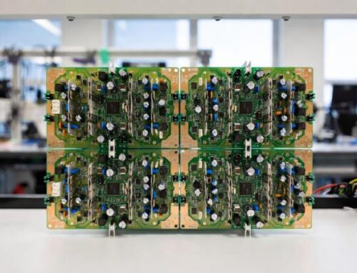
Printed Circuit Board Assembly(PCBA) Process

Printed Circuit Board Assembly Refine (PCBA)
Electronic products such as cellphones, TVS, even vehicles, and more usage a core printed circuit board. So, just how do you assemble a lot of little components into a full circuit card? This write-up will present the entire procedure of printed circuit board assembly.
PCBA Procedure Circulation
Printed circuit board assembly procedure refers to the certain operating steps and technological demands of PCB assembly, and its procedure includes PCB style and construction, material procurement, SMT spot, testing, and three-proof paint.
Step One: PCB Style and Fabrication
PCB layout is PCB designers depend upon the certain practical needs made, including PCB schematic and circuit layout design and drawing. After examining, set up a PCB factory for prototype and production.
Step Two: BOM Table Layout and Material Acquisition
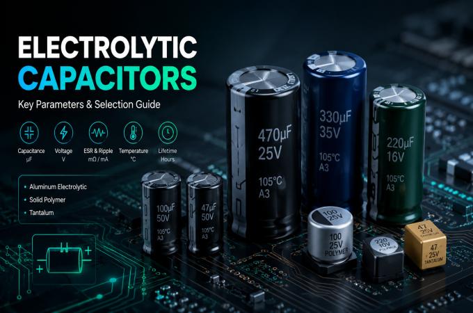
BOM (Bill of Products) is an in-depth document used by engineers to style and pick products. It specifies the item structure based upon item features and PCB drawings and exists in an information format.The procurement of products consists of the procurement of digital components and cables.
Tip 3: The SMT Spot
The SMT spot is a substantial part of the PCB assembly procedure, which connects the elements to the PCB substratum by welding. The welding forms consist of wave crest solder, re-flow soldering, and manual welding. Besides the selection of hands-on welding with rework, wave soldering, and re-flow welding are readily available. PCB must be cleaned sweep after welding. And they will be dried and sent for top quality screening.
1) Use Solder Paste:
Place the motherboard on a stainless-steel plate and use the solder paste appropriately and evenly to the solder pad externally of the circuit card.
Solder paste is a gray substance composed of many little steel rounds including 96.5% tin, 3% silver, and 0.5% copper. Solder paste is a combination of solder and flux. Change is a chemical that assists the solder thaw and stay with the surface.
2) SPI Discovery:
After completing solder paste printing, it needs to be checked utilizing an SPI equipment. To check is to verify the printing high quality of the solder paste and whether there exists tin leakage, tin less, and other troubles.
3) Spot:
After the solder paste is used, the robot will certainly put the surface area place elements on the ready PCB, after the BGA, IC, resistor, capacitor, and various other parts via the device devices will welded to the PCB surface via the maker devices.
4) Re-Flow Welding:
After the application of solder paste and surface area install parts, because of the solder paste having no strengthening result, the element is not very strong after placing, so the process of re-flow welding is needed to create the element to be solid on the board. In popular terms, it is taken into a heater, melting and cooling through high temperature. Parts are well on the board.
Step Four: Put the Through-Hole Element
Depending on the type of motherboard, the welding chosen approach is various. Besides the usual SMD, there are electroplated through-hole components or PHT components. The electroplated through openings are the holes via the circuit card. The signal is from one side of the board to the other with these holes. There is no attachment point for solder paste printing with openings. It calls for an unique soldering technique.
1) Manual Welding:
Utilizing hand-operated perforation welding.
2) Crest Welding:
Place the parts on the circuit card, use fluid flux on the component leads, and then pre-heat the motherboard to a specific temperature. Then, it is sent to the wave soldering equipment via a conveyor belt to melt the solder paste and develop solder joints. The elements are securely connected to the motherboard.
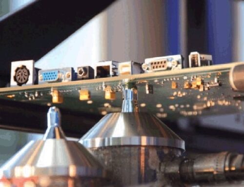
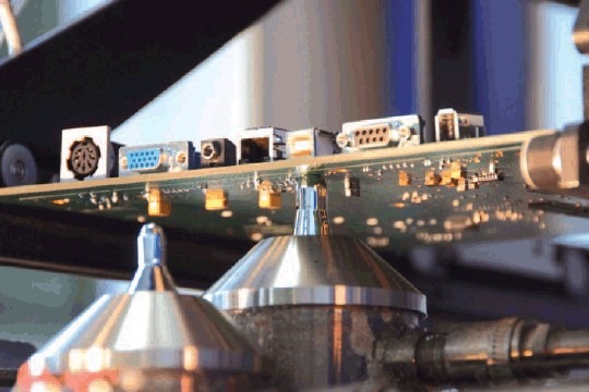
Step Five: PCB Cleansing
After the printed circuit board is set up, it must experience the cleansing action to tidy up the welding traces or impurities left over during the welding procedure. Deionized water or improvement solution is used to clean the motherboard, and deionized water is made use of to shoot the circuit card at heats and pressure. After cleaning, use a power jet to dry the circuit board and send it for a final product test.
Step Six: PCBA Examination
Printed circuit board setting up testing makes sure that the product is in the correct functioning problem, and some automated examinations are utilized to spot the PCB, more making certain PCB top quality and performance. The test consists of useful testing, burn-in screening, and dependability screening. The examination is the last and most critical action in the PCBA procedure and determines the success of the previous procedure steps. There are a number of detection approaches:
1) Visual Inspection:
For a few circuit boards, we can pick an Visual inspection. By the designer to check and make certain the high quality of the PCB.
2) Automatic Optical Inspection:
This method is suitable for massive PCBA inspection. The automated optical inspection machine uses high-performance electronic cameras to observe and detect where there is an issue with welding from different angles.
3) X-Ray:
Usage infrared to inspect the printed motherboard assembly internal layer for possible troubles.
4) In-Circuit Test System(ICT):
It primarily spots the open circuit, short circuit, and welding problem of all parts of the PCBA by speaking to the test points on the PCB layout with the test probe.The printer will certainly tell the user precisely which element is damaged or where the short circuit is located.
5) QC Manual Inspection:
According to the standard IPC-610 evaluation criterion, the completed board check to make sure 99.98% great product distribution.
6) QA Delivery Examination:
Strict inspection prior to shipment of products and scan code checks to avoid unqualified products from being shipped.
Step Seven: Apply Three Anti-Paint
Using conformal covering on the PCBA surface can avoid dampness and corrosion, hence extending the item’s service life. After the above steps are both finished, you can load and deliver.
Summary
As a whole, printed circuit board assembly is a facility and troublesome process. It requires to be detailed. Each step is important. In actual procedure, relying on the requirements of consumers, PCB assembly manufacturer require according to the design requirements of clients to plan a collection of assembly processes to make certain the high quality and function of items.
