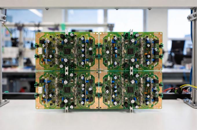
Welding Bridging Issues During PCBA Processing

printed circuit board assembly(PCBA) manufacturers, as the size of
electronic devices continues to shrink, are faced with a whole new set of challenges. It is certain that
the trend toward smaller and more compact electronic products will continue. Smart PCBA manufacturers
are actively working to address these challenges in order to adapt to the changes and prepare for future
development. The problem of welding bridges is a major challenge that all in our industry will have to
overcome.
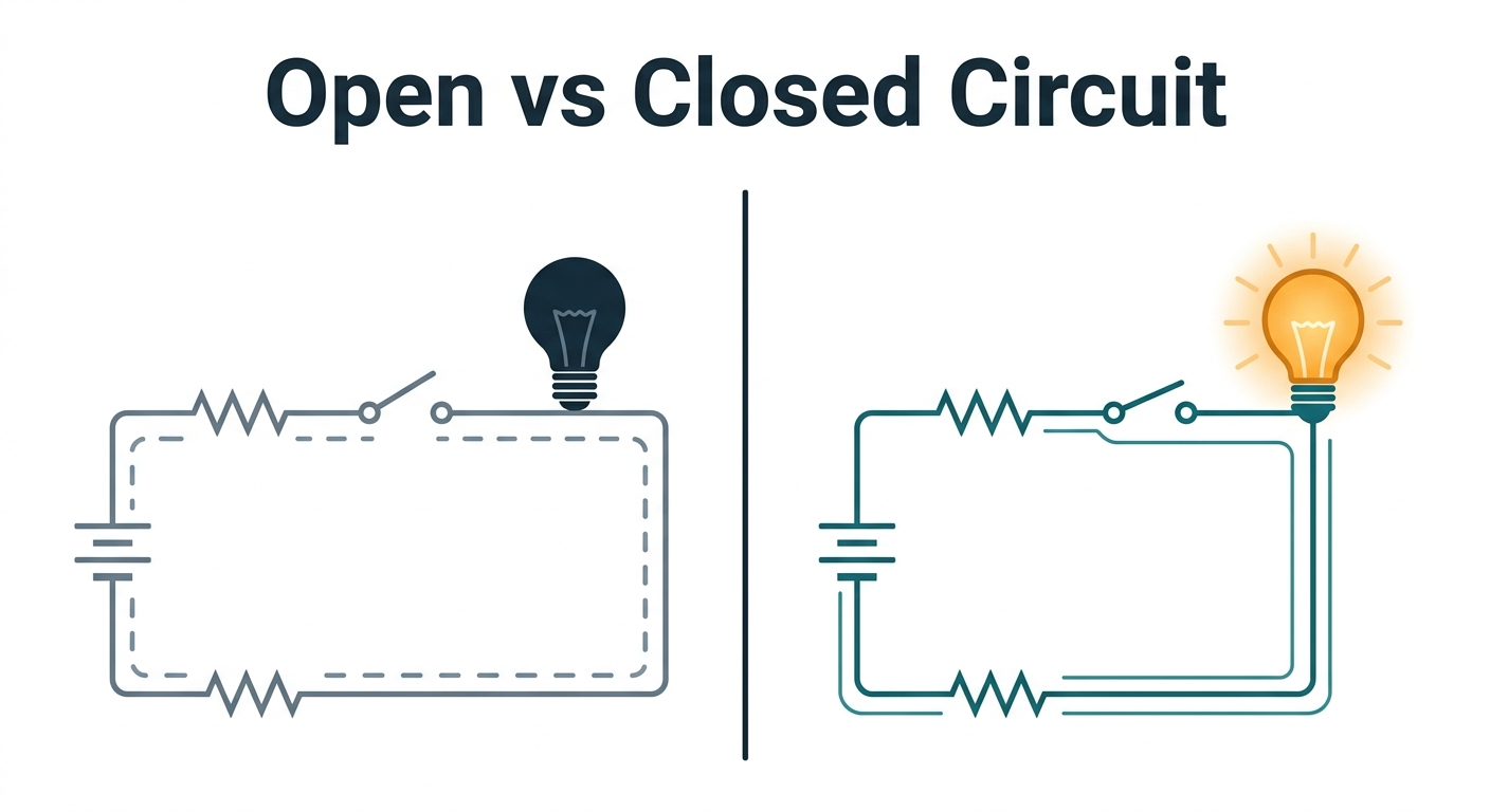
A common defect is welding bridging. It occurs when the welding flows into connectors,
causing a short circuit or “bridge”. It is not always obvious when welding bridging happens…
but it can lead to serious damage of electronic components or devices. Bridging can happen at many
points during the manufacturing process. Bridging can also occur when the welding paste is being
printed. This occurs when the additional welding paste is squeezed between printed board and the steel
mesh. Other factors can cause it, such as PCB manufacturing issues, pressure while placing electronic
components, incorrect settings in the reflow-oven, etc. Bridging can be caused by board design issues,
too much paste or other problems. It is a major headache for PCBA producers.
Reduce Welding Bridges
In order to reduce welding bridging we must acknowledge that there is not a single method for
eliminating it. Welding bridging can be caused by many factors. We have found some ways to reduce
welding bridging.
1) Adjust the Board Design
It is not always feasible. PCBA contract manufacturers may not have the final say on board design. When
possible, this is the best way to reduce bridging. This is especially true when adjusting the area and
aperture ratio. To prevent welding bridges, it is possible to add welding mask barriers between pads
with fine pitches. The use of welding mask-defined pads, particularly in areas with narrow pitches such
as BGAs or LGAs, can prevent bridging.
2) Adjust the Reflow Profiles
The welding will have more time to reach its intended location if the dwell time is increased above the
liquidus. The welding will wet the lead and pad once they reach the same temperature. This will cause
the welding to flow to its intended location. The liquid welding will tend to flow towards the hotter
surface. The leads of electronic components have a lower thermal mass and due to increased airflow, they
can run hotter than welding pads. By increasing the soak time, the temperature will be evened out across
the component. This will reduce the tendency for welding to flow towards hotter surfaces.

(3) Reduce the Risk of Noncontact Welding Paste Printing
You can also adjust the board design to eliminate factors that cause poor printed contact. You can
adjust the board to eliminate factors which cause poor printed contacts. The legend marking ink can
cause debonding if it is placed next to the pads that are defined by the mask. This can increase the
amount welding paste.
(4) Reduce the Quantity of Welding Paste, or Reduce Component Lead Size
By modifying the stencil, you can reduce the amount of paste or the location on the pad. Bridging can be
a problem when the welding paste reaches areas it shouldn’t.
Assembly with larger leads can reduce the likelihood of welding flowing in between them. The larger the
component, the more welding it can hold. This prevents the welding from flowing between the pads. The
pad is designed for long leads while the component assembly is shorter. This is a common cause of
welding bridges. The pad must be wetted in a large area, which reduces the amount of fluid that can flow
down the lead.
The thermal differences between gull-wing leads and other leads can be a challenge. During reflow weld,
welding paste may pool and cause bridges. You can adjust the stencil to lessen the amount of paste that
is printed on the pad.
Engineering Support
Need help with bridging problems? Need help with welding issues?
There are more resources available to avoid SMT defects caused by welding bridges
Need more help? Our field application engineers have written technical papers that provide additional
insight and guidance to solve issues that reduce SMT processing yields. This includes bridging.
PCBA manufacturers are able to save time and money by using root cause analysis when designing stencils.
They can also improve the reliability of their products and reduce first-pass defects. Yield is a
combination of cost, reliability and delivery. These are key factors in achieving an effective and
profitable PCBA process.
The main reason for yield problems in PCBA manufacturing is welding paste printing… This phenomenon is
becoming worse as the trend towards smaller form factors continues.
Orinew Technology: This article examines the defects that impact SMT yield and their causes. It
also investigated the impact of weight and surface treatment on the printability

