What Is Making Use of a Circuit Board Panel (PCB Panel)?

What is a PCB Panel?
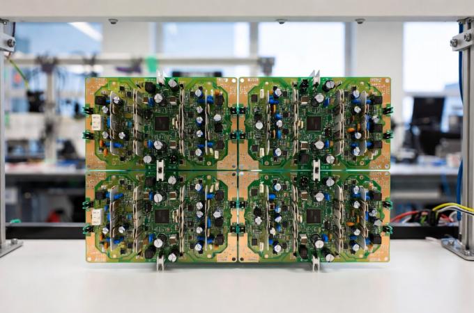
Printed circuit board panel connects two or more PCB devices to develop a large PCB board and has many
applications and advantages.
Benefits of PCB Panel
A.Improve SMT Manufacturing Efficiency
Lots of PCB systems turn into one large PCB board at that time and can minimize the variety of board
transfers and cycle regularity.
That permits even more circuit card items at the same time and boosts general manufacturing performance,
reducing the price of PCB board. It is important for makers that produce digital products in big
quantities.
B.Maximize Board Use
By splicing small-sized or irregular-shaped PCB systems, the area of the motherboard can be fully
utilized, reducing waste and production expenses. It is an important factor to consider for affordable
production procedures.
C.Reduce Manufacturing Difficulty
Streamlining the complex PCB framework comes to be a much more simplified structure, and can reduce the
technological problem in the production process.
It is also crucial to making certain product high quality and boosting production efficiency.
PCB Panel Layout Process

During the printed circuit board panel style procedure, in addition to thinking about the fundamental
elements, you likewise focus on other details to ensure the final layout item conforms to needs.
First, the comprehensive factor to consider of item features needs to be a lot more
in-depth, including exact analysis of circuit format, signal transmission, and power intake.
That assists stay clear of complicated circuit structures creating function deterioration and guarantees
that the whole PCB panelization system can operate stably and accurately.
On top of that, board usage and manufacturing effectiveness likewise need to be
completely enhanced.
When picking the number and approach of paneling, we ought to take into consideration the ability and
effectiveness of the production line to guarantee that the motherboard panel plan does not introduce
additional production concerns.
Superb setup and design can additionally minimize material waste and have a positive effect on
environmental management and lasting growth.
In the item dependability and performance facet, special demands to concentrate on the influence of
panelization on circuit stability and signal integrity.
Via sensible layout can stay clear of signal line crossover and disturbance, and can preserve the
function of the PCB panelization to the best degree.
The style of high-frequency circuits and sensitive parts calls for more exact analysis and format to
guarantee that the item can run stably and reliably under numerous functioning conditions.
Additionally, it is also crucial to take into consideration the handling problem and
production expense of SMT manufacturing.
The PCB panel plan must coordinate with the SMT production process to stay clear of introducing
unnecessary process troubles.
At the same time, a thorough assessment of manufacturing expenses, including product
expenses, labor expenses, and equipment expenses, need to make sure that the circuit card panel style is
cost-efficient and viable.
Throughout the whole PCB panel layout process, we interact very closely with the production line to make
certain that the style strategy conforms to item requirements and can create products at the same time.
Summary
To summarize, printed circuit card panel layout is a complex and comprehensive process that requires
engineers to consider adequately at various degrees.
Via careful layout, we can not only improve production effectiveness and reduce prices, but additionally
ensure that items get to ideal integrity and efficiency.
Today, as innovation and manufacturing remain to advancement, the optimized style of PCB panels will
play an essential duty in promoting electronic item producing to a greater degree.
